![]()
THine Value Extending MIPI Transmission with V-by-One HS: Simplifying SerDes Chipset Selection for Embedded Cameras (Sub-Link Part)
2022.08.22
- Article
- Use Case
In the previous article, we introduced the design guide for the Main-Link. This time, we will delve into the design guide for the Sub-Link, which is used to transmit control signals.
What is the Sub-Link?
Before going into the details of the Sub-Link, let us first clarify the overall concept of the Main-Link and Sub-Link using the V-by-One® HS-based transmitter IC, the THCV241A, as an example (see Fig. 1). The THCV241A is an IC that converts the MIPI® CSI-2 signal output from a camera module into a V-by-One HS signal. The Main-Link refers to the path that transmits the V-by-One HS signal. Meanwhile, the THCV241A also includes control signal interfaces for I2C and general-purpose input/output (GPIO). The path used to transmit these signals between the transmitter IC and receiver IC is known as the Sub-Link. By utilizing the Sub-Link's functionality, users can not only transfer image data through the transmitter and receiver ICs but also implement more complex systems, such as powering on or off the camera module from the SoC, resetting it, or turning on an LED. When using the Sub-Link functions, the Sub-Link must also be connected to the receiver IC, just like the Main-Link.
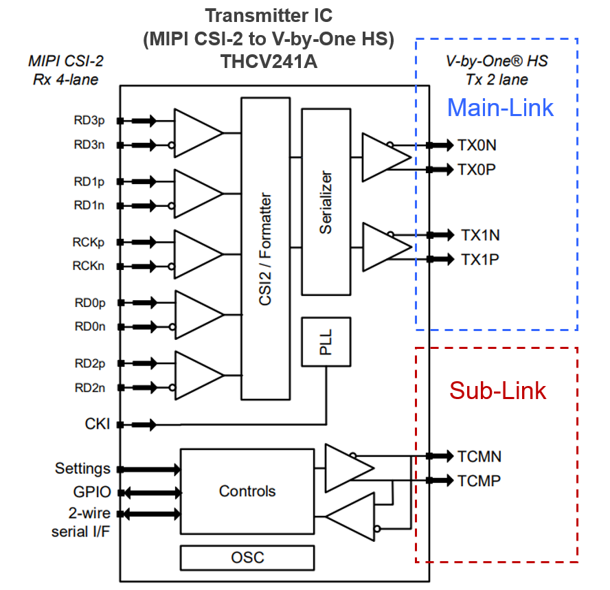

Fig. 1 Block diagram of the THCV241A transmitter IC
Sub-Link: Mastering the Through GPIO and Register GPIO
As mentioned earlier, signals such as I2C and GPIO can be transmitted via the Sub-Link. There are two types of GPIO control methods: Through GPIO and Register GPIO. Device manufacturers (users) must master the use of both control methods to design the optimal system.
First, Through GPIO is a method where the transmitter and receiver ICs between the SoC and the camera module act as if they are not present, allowing the SoC to control the camera module directly. This enables long-distance transmission without requiring a change to the SoC configuration. Furthermore, since the transmitter and receiver ICs simply relay signals, the SoC can control the camera module in real time.
However, in the combination of THCV241A and THCV242A, there is limitation of up to four GPIO pins (GPIO0, GPIO1, GPIO2, and GPIO3) usable as Through GPIO, with only two lines available in each direction (upstream and downstream) (see Fig. 2). Therefore, if the number of connected camera modules increases or the number of elements to control via GPIO grows, control using only Through GPIO may become difficult.

This is where Register GPIO comes into play to handle control operations not covered by Through GPIO. Register GPIO allows the SoC to rewrite the registers of the receiver and transmitter ICs via the I2C bus at desired points in time to perform the intended control (see Fig. 3). This enables the construction of more complex system configurations beyond the limitations of Through GPIO.

However, two considerations require attention when using Register GPIO compared to Through GPIO. The first is the need to add new specifications for Register GPIO control and the SoC’s control software. The GPIO pins must be controlled by rewriting the contents of each register via the I2C bus each time, in accordance with the SoC’s timing. The second is the inferior real-time performance. Since the transmitter IC and receiver IC operate based on the rewritten register values, latency occurs. System design engineers must evaluate their systems while considering the limitations and characteristics of both Through GPIO and Register GPIO.
First, Through GPIO is a method where the transmitter and receiver ICs between the SoC and the camera module act as if they are not present, allowing the SoC to control the camera module directly. This enables long-distance transmission without requiring a change to the SoC configuration. Furthermore, since the transmitter and receiver ICs simply relay signals, the SoC can control the camera module in real time.
However, in the combination of THCV241A and THCV242A, there is limitation of up to four GPIO pins (GPIO0, GPIO1, GPIO2, and GPIO3) usable as Through GPIO, with only two lines available in each direction (upstream and downstream) (see Fig. 2). Therefore, if the number of connected camera modules increases or the number of elements to control via GPIO grows, control using only Through GPIO may become difficult.
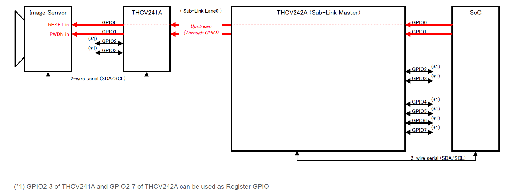
Fig. 2 System configuration using only Through GPIO
This is where Register GPIO comes into play to handle control operations not covered by Through GPIO. Register GPIO allows the SoC to rewrite the registers of the receiver and transmitter ICs via the I2C bus at desired points in time to perform the intended control (see Fig. 3). This enables the construction of more complex system configurations beyond the limitations of Through GPIO.
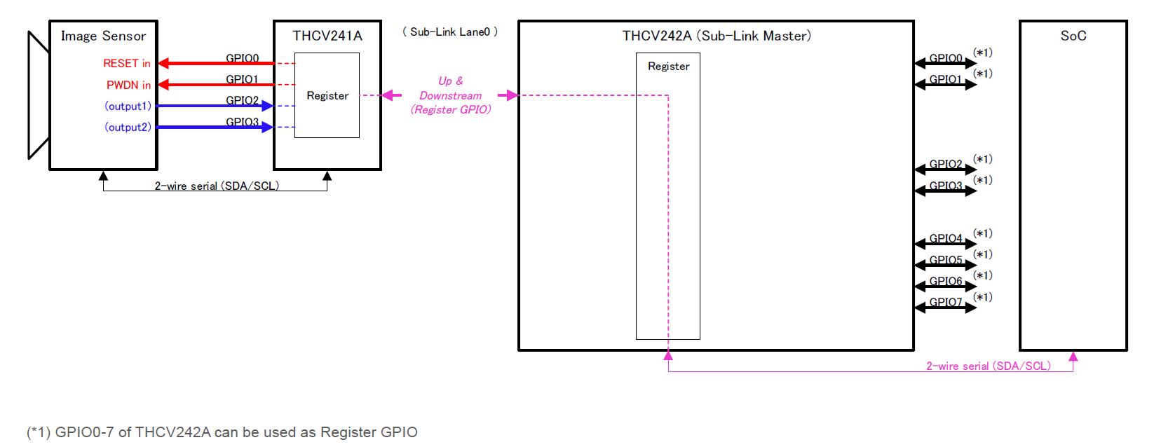
Fig. 3 Example of control using Register GPIO
However, two considerations require attention when using Register GPIO compared to Through GPIO. The first is the need to add new specifications for Register GPIO control and the SoC’s control software. The GPIO pins must be controlled by rewriting the contents of each register via the I2C bus each time, in accordance with the SoC’s timing. The second is the inferior real-time performance. Since the transmitter IC and receiver IC operate based on the rewritten register values, latency occurs. System design engineers must evaluate their systems while considering the limitations and characteristics of both Through GPIO and Register GPIO.
EXTSYNC: Synchronizing Multiple Cameras
This design guide for the Sub-Link concludes by discussing a function called EXTSYNC (see Fig. 4). EXTSYNC is used to synchronize the operation of two camera modules and an SoC, such as in stereo camera systems. There are two ways to achieve this. One method is to distribute a synchronization signal generated by the SoC to two camera modules via Through GPIO. The other method is to generate the sync signal using a sync generator built into the receiver IC, distribute it to two camera modules via Through GPIO, and simultaneously send it to the SoC via the dedicated EXTSYNC pin. Either method can be used to build a synchronized multi-camera system.
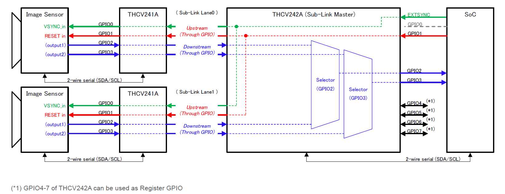

Fig. 4 Building a multi-camera synchronization system using EXTSYNC
The Interface Itself Does Not Add Value
Together with the previous Main-Link overview, we introduced two design guides aimed at reducing the time and effort required for system design. For electronic devices with camera modules, the interface itself does not add value. We hope the time and effort saved by using these two design guides can be redirected toward creating true added value.
Related Contents
- What is the High-speed Interface Standard MIPI? Going Beyond the Boundaries of Mobile Devices to Automotive Applications
- SerDes Starter Kit for Embedded Cameras Significantly Reduces Cable Extension Design Time for MIPI Cameras
- Extending MIPI Transmission with V-by-One HS: Simplifying SerDes Chipset Selection for Embedded Cameras (Main-Link Part)