![]()
THine Value What is the High-speed Interface Standard MIPI? Going Beyond the Boundaries of Mobile Devices to Automotive Applications
2025.08.19
- Article
- Column
A variety of high-speed interface technologies are currently used in electronic devices. These include USB, Thunderbolt, MIPI, HDMI, DisplayPort, Serial ATA (SATA), and LVDS.
One of these high-speed interface technologies is highly prevalent with relatively low consumer awareness. And that high-speed interface technology is Mobile Industry Processor Interface (MIPI). MIPI is a high-speed interface standard established in 2008. Even with this relatively established history, most general consumers are familiar with USB, Thunderbolt, and HDMI, but not MIPI.
Why is that? MIPI is used inside mobile devices such as cellular phones and smartphones as an interface for image signals between the camera and the SoC or between the SoC and the display. In other words, MIPI does not have an output outside the device that the average consumer can directly touch. There is no real way for a consumer to know.
MIPI is rapidly spreading and expanding in markets other than mobile applications. MIPI, which has been meeting the high-resolution requirements of cameras mounted on smartphones, has a wide variety of high-resolution compatible sensors. MIPI has been increasingly considered for embedded camera systems other than mobile applications in recent years due to the growing demand for higher resolution.
In this article, we are taking a deep dive into MIPI to understand its specifications and characteristics.
Starting as a Mobile-specific Standard
MIPI achieves high data transmission rates using low-voltage amplitude differential transmission technology such as LVDS. However, there are some points to note. That is, no single physical layer (PHY) standard defines data transmission rates and methods. In fact, there are multiple physical layer standards for MIPI.
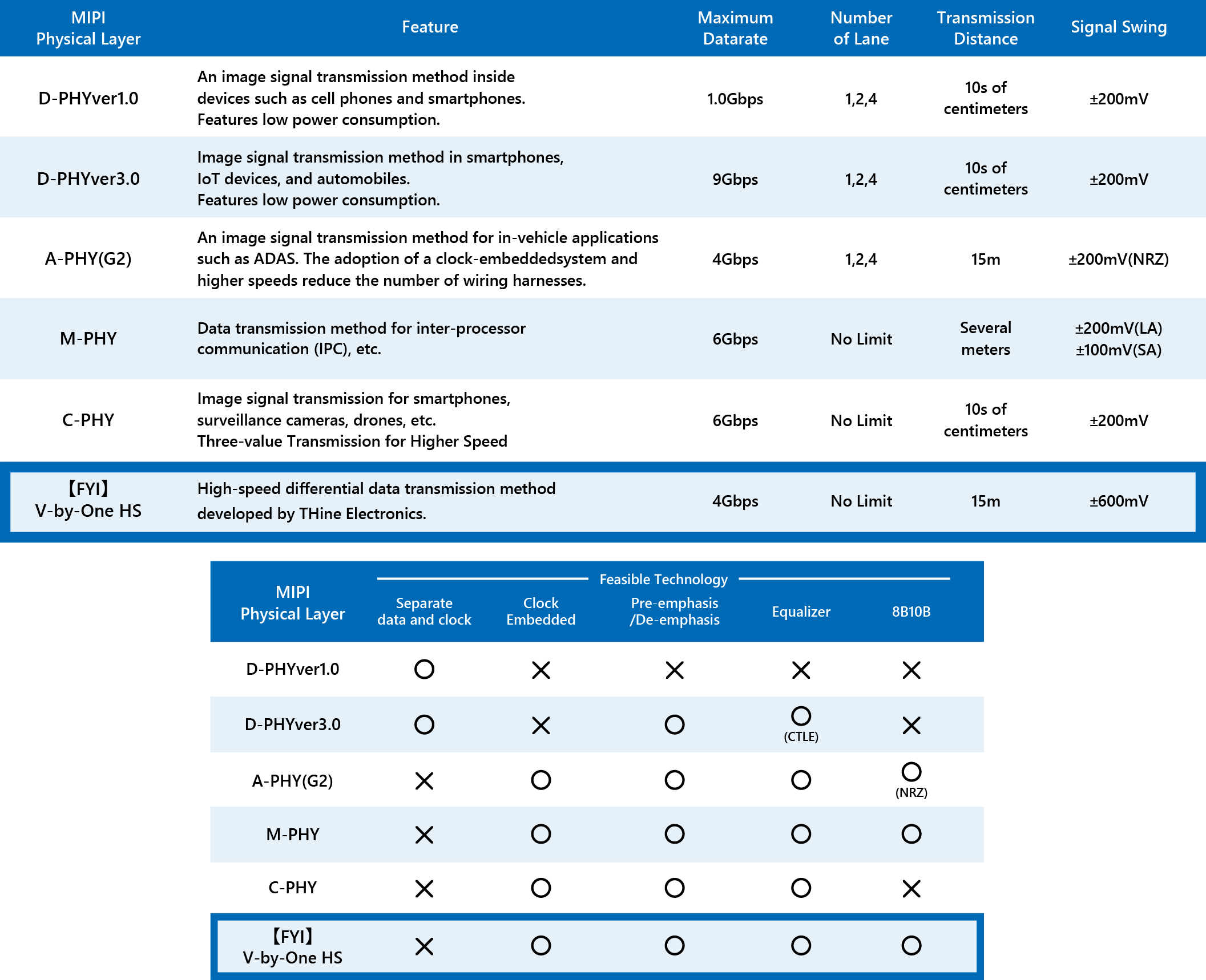
The first physical (PHY) layer standard established in 2008 was D-PHY v1.0, with a maximum data transmission rate of 1 Gbps per lane (Table 1). D-PHY v1.0 is a standard optimized for mobile devices for target applications, with two optimization points: simplicity and low power consumption.
 The first, simplicity, was achieved by adopting a separated clock transmission method in which data and clock signals are transmitted on separate signal lines. The separated clock transmission method has the challenge that as the transmission distance increases, the timing at which the data and clock signals arrive at the receiver IC becomes misaligned due to skew caused by differences in signal line lengths and characteristics. In the worst cases, transmission errors may occur. However, for signal transmission inside mobile devices, sending signals over such long distances is unnecessary. In practice, the distance transmitted with D-PHY v1.0 is in the tens of centimeters. It can be said that this standard was developed with the decision to adopt the separated clock transmission method, prioritizing simplicity over transmission distance.
The second point to note, low power consumption, was achieved by limiting the voltage amplitude of differential signals to ± 200 mV. Since LVDS is ± 350 mV, the voltage amplitude is calculated to be reduced to 4/7th of LVDS to D-PHY v1.0. This is the amount of power consumption reduction that can be achieved. Of course, the smaller the voltage amplitude, the shorter the distance over which data signals can be transmitted. However, as mentioned above, MIPI is intended for signal transmission inside mobile devices and does not require data to be sent over long distances. This shorter distance of required transmission was allocated to reducing power consumption.
The first physical (PHY) layer standard established in 2008 was D-PHY v1.0, with a maximum data transmission rate of 1 Gbps per lane (Table 1). D-PHY v1.0 is a standard optimized for mobile devices for target applications, with two optimization points: simplicity and low power consumption.
Table 1 MIPI physical layer standards
The second point to note, low power consumption, was achieved by limiting the voltage amplitude of differential signals to ± 200 mV. Since LVDS is ± 350 mV, the voltage amplitude is calculated to be reduced to 4/7th of LVDS to D-PHY v1.0. This is the amount of power consumption reduction that can be achieved. Of course, the smaller the voltage amplitude, the shorter the distance over which data signals can be transmitted. However, as mentioned above, MIPI is intended for signal transmission inside mobile devices and does not require data to be sent over long distances. This shorter distance of required transmission was allocated to reducing power consumption.
Emerging Automotive Applications for Physical Layer Standards
As mentioned earlier, the MIPI standard has multiple physical layer standards. For example, D-PHY v1.0 has seen upgrades and is currently on D-PHY v3.0. D-PHY v3.0 uses the same differential transmission signal amplitude and separated clock transmission method as D-PHY v1.0, but by adding de-emphasis and equalizer technologies, the maximum data transmission speed has been increased to 6 Gbps per lane.
In addition, there are two other standards, C-PHY and M-PHY, which change the transmission method from the separated clock transmission method to the clock-embedded method. C-PHY is a physical layer standard for smartphones, surveillance cameras, and drones. The most significant of its features is that the maximum data transmission speed has been increased to 6 Gbps per lane by adopting a three-level transmission method in addition to the clock-embedded method.
M-PHY is a physical layer standard for Inter-Processor Communication (IPC) in mobile devices. By applying equalizer technology and 8B10B modulation technology, the maximum data transmission rate has been increased to 6 Gbps per lane, similar to C-PHY.
D-PHY v3.0, C-PHY, and M-PHY are all aimed at mobile devices, which are the target applications for the MIPI standard. The standard can be said to have been upgraded time and time again to support new uses within the scope of mobile devices by adopting new transmission technologies and increasing its maximum data transmission speeds.
However, in September 2020, a standard was established that deviates significantly from this trend. That is in reference to A-PHY, a physical layer standard for automotive applications. This is intended for data transmission applications between cameras and displays inside automobiles. While this is a category of "high-speed data transmission standards within devices," the scope of "mobile devices" has gone far beyond this category.
The required transmission distance will naturally increase significantly if the application changes from mobile devices to automobiles. Therefore, in addition to the clock-embedded method, A-PHY uses de-emphasis, equalizer, and 8B10B modulation technology to extend the transmission distance to a maximum of 15 meters. The maximum data transmission rate per lane is 2 Gbps. In the future, the standard is planned to receive an increase in maximum data transmission speed to a maximum of 6 Gbps per lane while maintaining a maximum transmission distance of 15 meters.
Solving the Problem with V-by-One HS
Thus, the MIPI physical layer standard has significantly evolved from the original D-PHY v1.0. However, even at this point, a few applications still use the early forms of D-PHY.
The maximum data transmission rate of D-PHY is 1.0 Gbps for v1.0 and 1.5 Gbps for v1.1, which would be a high enough data transmission rate for general use. However, more than a transmission distance of several tens of centimeters is required for some applications. For example, a camera module with MIPI D-PHY output (MIPI camera) is used to build an industrial IoT system. For crop monitoring in an orchard, the camera module would be mounted on a fruit tree trellis and connected to a SoC board on the ground with a cable. Currently, with its D-PHY physical layer standard, MIPI needs more transmission distance.
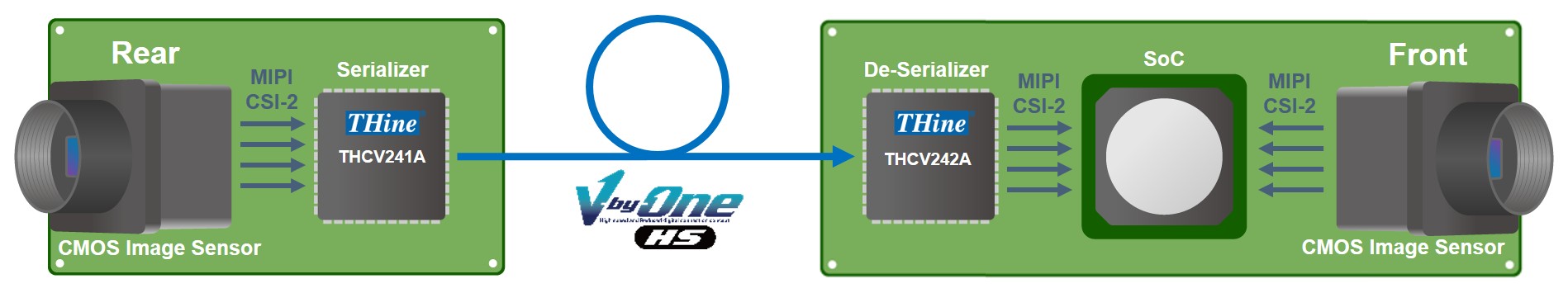
One way to solve this transmission distance challenge is to use V-by-One HS, a high-speed interface technology. Here's how to use V-by-One HS: First, a transmitter IC connected to the camera module converts MIPI signals compatible with D-PHY to V-by-One HS signals. This signal is then sent over an Ethernet cable or similar medium, and a receiver IC connected to a remote SoC board converts the V-by-One HS signal back to a MIPI signal (Fig. 1).
V-by-One HS, like MIPI, is a high-speed interface technology using low-voltage amplitude differential transmission technology. However, unlike MIPI, it is not specific to mobile devices and is a general-purpose high-speed interface technology. The voltage amplitude is ± 600 mV, and the clock-embedded method is used. In addition, because de-emphasis and equalizer technologies are used, the maximum data transmission speed is as high as 4 Gbps per lane, and the maximum transmission distance is as long as approximately 15 meters. Therefore, the transmission distance problem faced by MIPI supporting D-PHY can be solved in one fell swoop.
The maximum data transmission rate of D-PHY is 1.0 Gbps for v1.0 and 1.5 Gbps for v1.1, which would be a high enough data transmission rate for general use. However, more than a transmission distance of several tens of centimeters is required for some applications. For example, a camera module with MIPI D-PHY output (MIPI camera) is used to build an industrial IoT system. For crop monitoring in an orchard, the camera module would be mounted on a fruit tree trellis and connected to a SoC board on the ground with a cable. Currently, with its D-PHY physical layer standard, MIPI needs more transmission distance.
One way to solve this transmission distance challenge is to use V-by-One HS, a high-speed interface technology. Here's how to use V-by-One HS: First, a transmitter IC connected to the camera module converts MIPI signals compatible with D-PHY to V-by-One HS signals. This signal is then sent over an Ethernet cable or similar medium, and a receiver IC connected to a remote SoC board converts the V-by-One HS signal back to a MIPI signal (Fig. 1).

Fig. 1 V-by-One HS application example (dash cam)
V-by-One HS, like MIPI, is a high-speed interface technology using low-voltage amplitude differential transmission technology. However, unlike MIPI, it is not specific to mobile devices and is a general-purpose high-speed interface technology. The voltage amplitude is ± 600 mV, and the clock-embedded method is used. In addition, because de-emphasis and equalizer technologies are used, the maximum data transmission speed is as high as 4 Gbps per lane, and the maximum transmission distance is as long as approximately 15 meters. Therefore, the transmission distance problem faced by MIPI supporting D-PHY can be solved in one fell swoop.
Releasing an Easy-to-use Development Kit
Currently, THine Electronics began selling the MIPI Camera SerDes Starter Kit in February 2023, which can significantly increase the signal transmission distance of MIPI cameras. When using this starter kit, please use a combination of the SerDes set THEVA24-RJ45-SET-V1, the specified grabber board THEVA-GRABBER-V1, and a compatible camera module (Fig. 2).
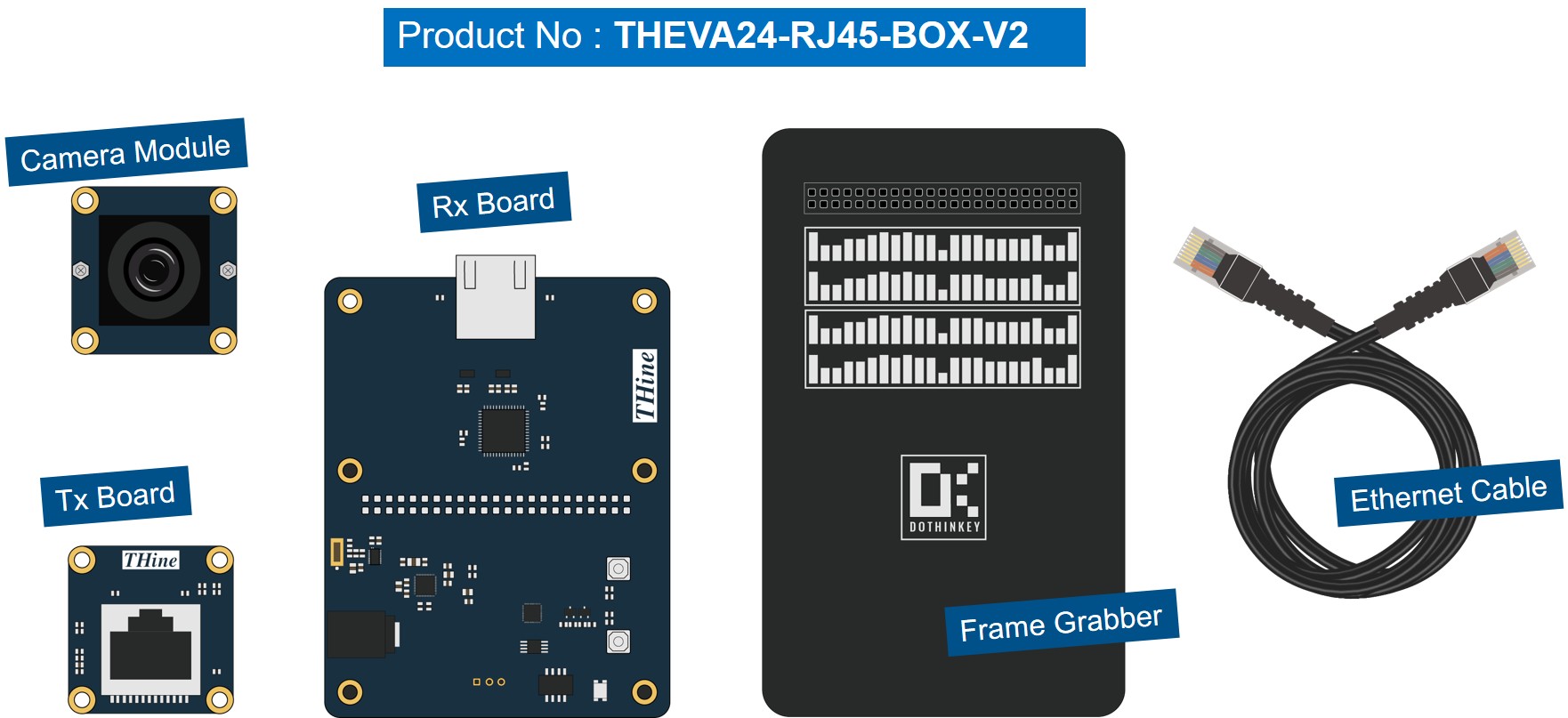
The THEVA24-RJ45-SET-V1 includes a Tx board on the camera side, an Rx board on the grabber board side, and an Ethernet cable as a set. The Tx and Rx boards are equipped with THine Electronics' MIPI interface conversion SerDes chip sets, THCV241A-P (transmitter IC) and THCV242A-P (receiver IC).
For more information on this development kit, please click here.

Fig. 2 Starter kit set contents and grabber board
The THEVA24-RJ45-SET-V1 includes a Tx board on the camera side, an Rx board on the grabber board side, and an Ethernet cable as a set. The Tx and Rx boards are equipped with THine Electronics' MIPI interface conversion SerDes chip sets, THCV241A-P (transmitter IC) and THCV242A-P (receiver IC).
For more information on this development kit, please click here.
Multiple ICs available for MIPI Distance Extension
Currently, THine Electronics offers seven products, including transmitter ICs that convert MIPI CSI-2 signals compliant with the D-PHY standard into V-by-One HS signals for transmission and receiver ICs that convert received V-by-One HS signals into MIPI CSI-2 signals compliant with the D-PHY standard for output. Below is additional information regarding each of these ICs.
The THCV243 features a small footprint of 2.9 mm x 2.1 mm using the CSP35 package. This makes it suitable for small cameras. It has a maximum of four input lanes for MIPI CIS-2 signals and one output lane for V-by-One HS. The maximum data transmission rate for MIPI CSI-2 signals is 1.2 Gbps, and the maximum for V-by-One HS signals is 4 Gbps.
The four receiver ICs are the THCV242A, THCV242A-P, THCV244A, and THCV244A-QP. Both the THCV242A and THCV242A-P have four lanes of MIPI CSI-2 signal input and two lanes of V-by-One HS signal output. Among these receiver ICs, the maximum data transmission rate for V-by-One HS signals is the same at 4 Gbps, but the maximum data transmission rate for MIPI CSI-2 signals is different. The THCV242A has a maximum of 1.2 Gbps, and the THCV241A-P has a maximum of 1.5 Gbps.
The THCV244A and THCV244A-QP feature four lanes of V-by-One HS signal input. This makes these ICs suitable for applications where multiple cameras capture images, such as a surrounding view of an automobile. These ICs also have a maximum data transmission rate for V-by-One HS signals of 4 Gbps, but the maximum data transmission rate for MIPI CSI-2 signals is 1.2 Gbps for THCV244A and 1.49 Gbps for THCV244A-QP.
All four of these use the QFN64 package with a footprint of 9 mm x 9 mm.
End
Table 2 Transmitter/receiver ICs supporting V-by-One HS and MIPI
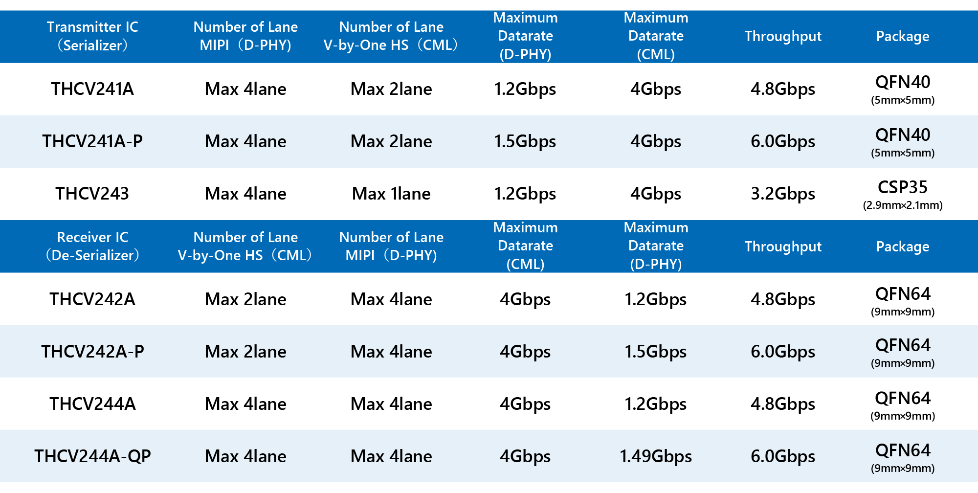
The three transmitter ICs are the THCV241A, THCV241A-P, and THCV243. Both the THCV241A and THCV241A-P have four lanes of MIPI CSI-2 signal input and two lanes of V-by-One HS signal output. Among these transmitter ICs, the maximum data transmission rate for V-by-One HS signals is the same at 4 Gbps, but the maximum data transmission rate for MIPI CSI-2 signals is different. The THCV241A has a maximum of 1.2 Gbps, and the THCV241A-P has a maximum of 1.5 Gbps. Both of these use the QFN40 package with a mounting area of 5 mm x 5 mm.
The THCV243 features a small footprint of 2.9 mm x 2.1 mm using the CSP35 package. This makes it suitable for small cameras. It has a maximum of four input lanes for MIPI CIS-2 signals and one output lane for V-by-One HS. The maximum data transmission rate for MIPI CSI-2 signals is 1.2 Gbps, and the maximum for V-by-One HS signals is 4 Gbps.
The four receiver ICs are the THCV242A, THCV242A-P, THCV244A, and THCV244A-QP. Both the THCV242A and THCV242A-P have four lanes of MIPI CSI-2 signal input and two lanes of V-by-One HS signal output. Among these receiver ICs, the maximum data transmission rate for V-by-One HS signals is the same at 4 Gbps, but the maximum data transmission rate for MIPI CSI-2 signals is different. The THCV242A has a maximum of 1.2 Gbps, and the THCV241A-P has a maximum of 1.5 Gbps.
The THCV244A and THCV244A-QP feature four lanes of V-by-One HS signal input. This makes these ICs suitable for applications where multiple cameras capture images, such as a surrounding view of an automobile. These ICs also have a maximum data transmission rate for V-by-One HS signals of 4 Gbps, but the maximum data transmission rate for MIPI CSI-2 signals is 1.2 Gbps for THCV244A and 1.49 Gbps for THCV244A-QP.
All four of these use the QFN64 package with a footprint of 9 mm x 9 mm.
End
Related Contents
- MIPI Camera SerDes Starter Kit for an Embedded Camera System in Long Reach
- SerDes Starter Kit for Embedded Cameras Significantly Reduces Cable Extension Design Time for MIPI Cameras
- Extending MIPI Transmission with V-by-One HS: Simplifying SerDes Chipset Selection for Embedded Cameras (Sub-Link Part)
- Extending MIPI Transmission with V-by-One HS: Simplifying SerDes Chipset Selection for Embedded Cameras (Main-Link Part)
- Cable Extension Kit for Raspberry Pi Camera (THSER102A) Applications