- HOME
- Products / Interface
- LVDS
- THC63LVDF84B

Overview
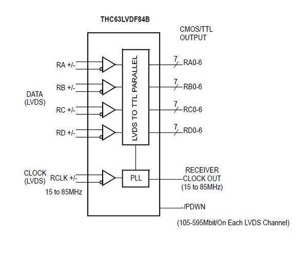
The THC63LVDF84B receiver converts the four LVDS data streams back into 24bits of CMOS/TTL data with wide VCC range(2.5 to 3.6V) and falling edge clock, suited to not only mid-sized LCD panels but also security camera systems, multi-function Printers, and tablet devices.
- LVDS to LVCMOS Conversion
- 4chs LVDS input
595Mbps/ch
LVDS input skew margin ±400ps - LVCMOS Parallel output
28bit/pixel
Clock Freq. 15 to 85MHz at 3.3V
based on Falling edge - Power Supply:3.3V
※2.5 to 3.0V available less than 70Mpixel /sec. - Package:TSSOP56
※Pin Compatible with THC63LVDF84A - Operating Temperature:-10 to 70℃
- Recommended Tx:
THC63LVDM83D
THC63LVDM87 - Recommended promotive replacement part
THC63LVDF84C
Go to FAQ for this product
Purchase Samples
Download documents
-
Data Sheet
-
IBIS Model
