InterfaceV-by-One® HSTHCV217

Overview
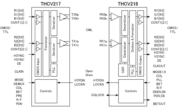
The THCV217 is designed to support video data conversion LVCMOS input signals into V-by-One®HS signals. This chip can transmit 32bit video data and 3bits control signals at a pixel clock frequency 20MHz to 85MHz. It has two high-speed data lane and, effective maximum serial data rate is 2.72Gbps/lane up to 4k2k/30Hz/16bits, 1080p/60Hz/30bits colors.
- LVCMOS to V-by-One®HS Conversion
- LVCMOS 2ports input
32bits/pixel - V-by-One®HS 2lanes output
3.4Gbps(effective rate 2.72Gbps)/lane - Power Supply:1.8/3.3V
- Package:TFBGA105
- Operation temp.:-20 to 85℃
- Recommended Rx:
THCV216
THCV218
| LVCMOS Input | V-by-One®HSOutput | LVCMOS Input Clock Frequency |
|---|---|---|
| 32bit | 1Lane | 20MHz to 85MHz |
| 32bit | 2Lane | 40MHz to 170MHz |
| 32bit x2 | 2Lane | 20MHz to 85MHz |
Go to FAQ for this product
Download documents
-
Data Sheet
-
Design Guide
-
Evaluation Board
