![]()
THine Value Sending Bundled GPIO and I2C with a Serial Transceiver: Two Changes with Significant User Benefits Explained
2025.09.29
- Article
- Column
This article is the second of a two-part series describing a serial tranceiver IC, IOHA:B. In Part 1 of this series, we described the features of the THCS253A/THCS254A and introduced the changes from the previous THCS251/THCS252, namely, I2C support on top of GPIO (general purpose I/O). We then explained the benefits that users can gain from this new product. In this second installment, we would like to describe the changes in more detail and introduce another change: the introduction of synchronous/asynchronous modes.
Freely Customizable I/O
The primary function of the successor THCS253A/THCS254A are to replace parallel transmission, which was sent on numerous signal lines, with serial transmission using only two pairs of differential lines. For example, 34 signal lines can be reduced to only four with our successor product. This gives us a line reduction of up to 88%. Moreover, this reduces the weight of the wiring cable, allowing an extension of the transmission distance. As part one of this series mentions, the benefits of these changes to users are significant.
However, these functions are identical to the conventional THCS251/THCS252 model and are not new. The THCS253A/THCS254A inherit these basic functions from the previous product while making two significant changes. These are I2C support in addition to GPIO, as mentioned at the beginning of this article, and the introduction of synchronous/asynchronous modes.
First, let us give you more details on the first change in this model, I2C support and GPIO. The meat of this change has already been briefly described in the first article. In other words, in addition to multiple GPIOs, one or two I2C systems can be bundled together for serial transmission. This bundling gives users an extremely significant advantage. The advantage is the ability to customize the I/O (input/output interface) with a high degree of freedom by rewriting internal registers using I2C.
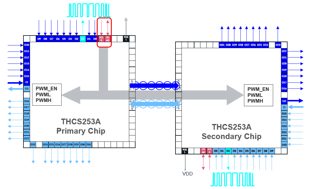
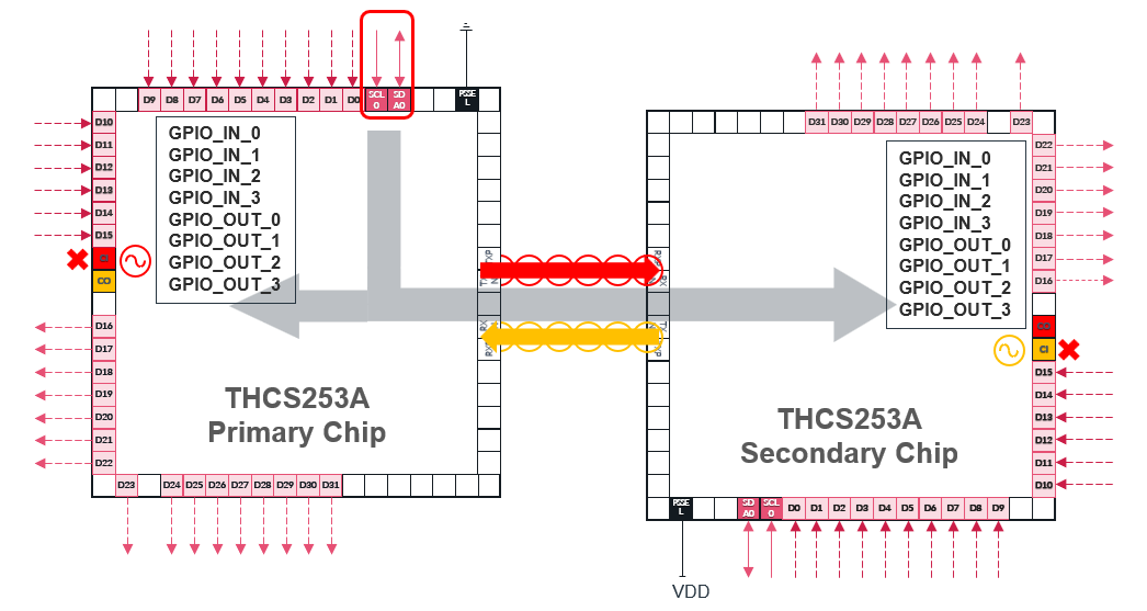
Let's get into the details. When applying the THCS253A/THCS254A to electronic devices, two identical chips (ICs) are prepared—one is designated as the primary chip and the other as the secondary chip—using PSSEL pins. The maximum number of GPIOs that can be handled is 32 for the THCS253A and 20 for the THCS254A. For example, the THCS253A has a default pin configuration of 16 GPIs (general-purpose inputs) and 16 GPOs (general-purpose outputs) (Fig. 1).
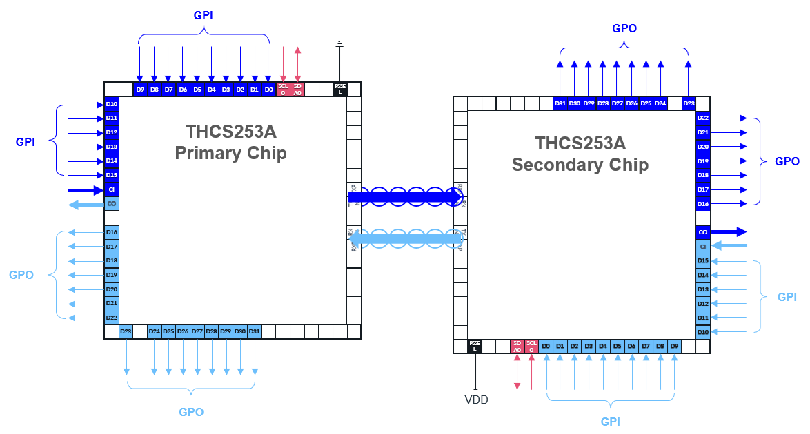 Fig. 1 Default I/O settings (THCS253A)
The user may freely set the number of these GPIs and GPOs. This flexibility stems from the fact that each pin can be designated as a GPI or GPO by rewriting the internal registers via I2C. Fig. 2 is a specific example of this phenomenon (an example in which each pin is assigned to a GPIO, I2S, SPI, or UART input/output).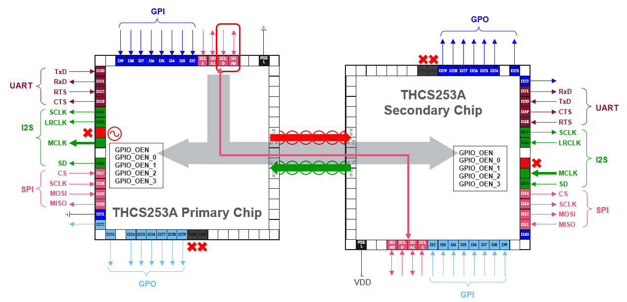
The conventional THCS251/THCS252 also allowed users to specify the number of GPIs and GPOs; however, these conventional models only allowed a selection of four levels indicating the ratio of the number of GPIs and GPOs. In other words, the degree of freedom to customize the I/O section is lower with the THCS251/THCS252 than in our the THCS253A/THCS254A.
Customizing the I/O section is highly effective when sudden design changes occur, such as adding new functions to the electronic equipment to be designed or when the design must be standardized in preparation for future model changes or additional functions. When design changes, model changes, or additional functions are implemented, the number of I/O pins may increase due to an increase in the number of circuits that allow for new functions, or the positioning of I/O pins may change. Conventional products did not allow a high degree of freedom in customizing the I/O section, and in some cases, hardware, such as signal transmission paths, had to be redesigned. However, by adopting our successor product, I/O can be customized with a high degree of freedom, allowing for highly flexible handling of design changes and additional functions. This flexibility gives users a higher chance of not needing to redesign hardware. This flexibility can help avoid situations where the design period is extended and design costs increase.
However, these functions are identical to the conventional THCS251/THCS252 model and are not new. The THCS253A/THCS254A inherit these basic functions from the previous product while making two significant changes. These are I2C support in addition to GPIO, as mentioned at the beginning of this article, and the introduction of synchronous/asynchronous modes.
First, let us give you more details on the first change in this model, I2C support and GPIO. The meat of this change has already been briefly described in the first article. In other words, in addition to multiple GPIOs, one or two I2C systems can be bundled together for serial transmission. This bundling gives users an extremely significant advantage. The advantage is the ability to customize the I/O (input/output interface) with a high degree of freedom by rewriting internal registers using I2C.
Let's get into the details. When applying the THCS253A/THCS254A to electronic devices, two identical chips (ICs) are prepared—one is designated as the primary chip and the other as the secondary chip—using PSSEL pins. The maximum number of GPIOs that can be handled is 32 for the THCS253A and 20 for the THCS254A. For example, the THCS253A has a default pin configuration of 16 GPIs (general-purpose inputs) and 16 GPOs (general-purpose outputs) (Fig. 1).
The user may freely set the number of these GPIs and GPOs. This flexibility stems from the fact that each pin can be designated as a GPI or GPO by rewriting the internal registers via I2C. Fig. 2 is a specific example of this phenomenon (an example in which each pin is assigned to a GPIO, I2S, SPI, or UART input/output).
Fig. 2 Customizing I/O by rewriting internal registers
The conventional THCS251/THCS252 also allowed users to specify the number of GPIs and GPOs; however, these conventional models only allowed a selection of four levels indicating the ratio of the number of GPIs and GPOs. In other words, the degree of freedom to customize the I/O section is lower with the THCS251/THCS252 than in our the THCS253A/THCS254A.
Customizing the I/O section is highly effective when sudden design changes occur, such as adding new functions to the electronic equipment to be designed or when the design must be standardized in preparation for future model changes or additional functions. When design changes, model changes, or additional functions are implemented, the number of I/O pins may increase due to an increase in the number of circuits that allow for new functions, or the positioning of I/O pins may change. Conventional products did not allow a high degree of freedom in customizing the I/O section, and in some cases, hardware, such as signal transmission paths, had to be redesigned. However, by adopting our successor product, I/O can be customized with a high degree of freedom, allowing for highly flexible handling of design changes and additional functions. This flexibility gives users a higher chance of not needing to redesign hardware. This flexibility can help avoid situations where the design period is extended and design costs increase.
Customizable Output Formats and Filters
In addition, the user can configure the output format and digital noise filter by rewriting internal registers utilizing I2C. Two output format options are available: push-pull and open drain. The digital noise filter can be set for each pin, and the user can also select the number of filter steps (filter order). However, the number of steps (filter order) cannot be set for each terminal. For example, if a user decides on three steps (third order), the filter step (filter order) applied to each terminal will all be the third step (third order).
The successor product has one I2C system by default, but we have prepared a mechanism that allows two GPIOs to be assigned to I2C to allow for two I2C systems by rewriting internal registers. Depending on the electronic device to be designed, in addition to the I2C system provided by the SoC, there may be another I2C system in modules/units, such as touch panels or near-field communication (NFC) that are purchased externally and incorporated. A mechanism that can increase the I2C count to two systems is helpful in such cases. Note that if two I2C systems (four signal lines) are used, the number of GPIOs for the THCS253A/THCS254A becomes 30 and 18, respectively.
The successor product has one I2C system by default, but we have prepared a mechanism that allows two GPIOs to be assigned to I2C to allow for two I2C systems by rewriting internal registers. Depending on the electronic device to be designed, in addition to the I2C system provided by the SoC, there may be another I2C system in modules/units, such as touch panels or near-field communication (NFC) that are purchased externally and incorporated. A mechanism that can increase the I2C count to two systems is helpful in such cases. Note that if two I2C systems (four signal lines) are used, the number of GPIOs for the THCS253A/THCS254A becomes 30 and 18, respectively.
Using Both Synchronous and Asynchronous Modes
Next, we discuss another significant change: introducing synchronous/asynchronous modes. Our conventional product, the THCS251/THCS252, could only be used in synchronous mode, but the THCS253A/THCS254A can be used in both synchronous and asynchronous modes. The user can select the mode in the secondary chip terminal settings.
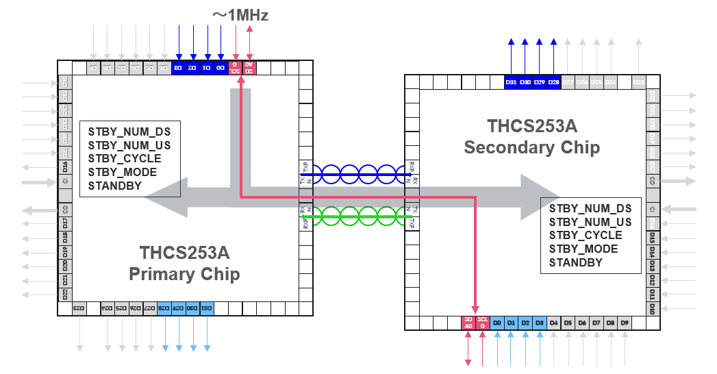
Synchronous mode is when the downlink from the primary chip to the secondary chip and the uplink from the secondary chip to the primary chip operate with the same reference clock signal. In other words, synchronous mode is when the frequency and phase of the downlink and uplink reference clock signals are precisely the same. In practice, the synchronous mode is when the uplink is operated by receiving a serial signal (Clock embedded 8B10B encoding signal) sent from the primary chip and using the clock signal extracted by the clock data recovery (CDR) circuit in the secondary chip (Fig. 3 and Fig. 4).
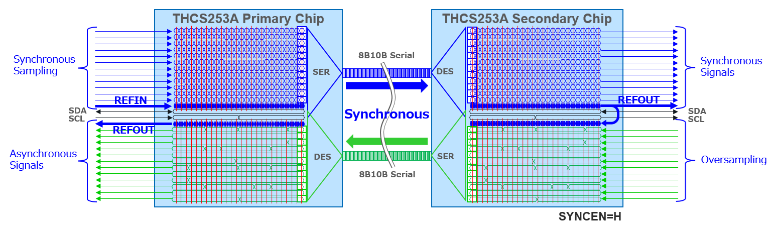 Fig. 3 Example of synchronous mode (with external input)
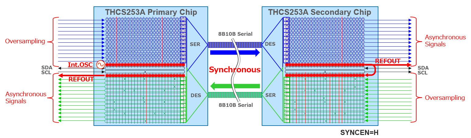 Fig. 4 Example of synchronous mode (for internal OSC)
On the other hand, asynchronous mode is when the downlink and uplink operate with different reference clock signal (Fig. 5 and Fig. 6). Even if the frequency of both reference clock signals is the same, if the phases are different, it will be asynchronous mode.
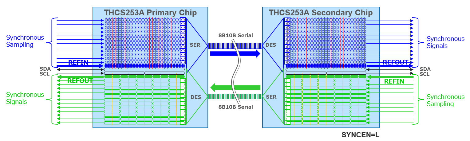 Fig. 5 Example of asynchronous mode (with external input)
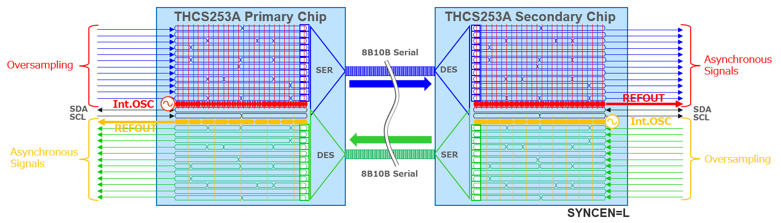 Fig. 6 Example of asynchronous mode (for internal OSC)
One advantage of synchronous mode is that it does not require a reference clock signal source to be supplied to the secondary chip. However, there are some disadvantages. The primary chip is the only one of the chips that can implement synchronous sampling of parallel signals. For the secondary chip, the reference clock signal used is extracted by the CDR circuit and is unrelated to the parallel signal to be captured, resulting in oversampling. A downlink with synchronous sampling can transmit high-speed image/video signals. In contrast, an uplink with oversampling cannot send high-speed image/video signals and can only transmit low-speed control signals.
Asynchronous mode was introduced to eliminate this disadvantage. Separate reference clock signals can be provided for the primary and secondary chips, allowing synchronous sampling of parallel signals on both. In other words, high-speed image/video signals can be sent through downlink and uplink.
There is one point to note here, however—the question being the method of supplying the reference clock signals to the primary and secondary chips. There are two supply methods. The first of these is to supply the reference clock signal from an external clock signal circuit. The other method is to supply the signal from the clock oscillation circuit (internal OSC) built into each chip. The former can allow common use together with the reference clock of the parallel signal to enable synchronous sampling. However, the latter cannot allow common use with the reference clock signal of the parallel signal because the internal OSC clock signal cannot be output externally, resulting in oversampling. Therefore, users need to select a reference clock signal supply method that matches the characteristics of the signals they wish to transit in the downlink and uplink.
Synchronous mode is when the downlink from the primary chip to the secondary chip and the uplink from the secondary chip to the primary chip operate with the same reference clock signal. In other words, synchronous mode is when the frequency and phase of the downlink and uplink reference clock signals are precisely the same. In practice, the synchronous mode is when the uplink is operated by receiving a serial signal (Clock embedded 8B10B encoding signal) sent from the primary chip and using the clock signal extracted by the clock data recovery (CDR) circuit in the secondary chip (Fig. 3 and Fig. 4).
On the other hand, asynchronous mode is when the downlink and uplink operate with different reference clock signal (Fig. 5 and Fig. 6). Even if the frequency of both reference clock signals is the same, if the phases are different, it will be asynchronous mode.
One advantage of synchronous mode is that it does not require a reference clock signal source to be supplied to the secondary chip. However, there are some disadvantages. The primary chip is the only one of the chips that can implement synchronous sampling of parallel signals. For the secondary chip, the reference clock signal used is extracted by the CDR circuit and is unrelated to the parallel signal to be captured, resulting in oversampling. A downlink with synchronous sampling can transmit high-speed image/video signals. In contrast, an uplink with oversampling cannot send high-speed image/video signals and can only transmit low-speed control signals.
Asynchronous mode was introduced to eliminate this disadvantage. Separate reference clock signals can be provided for the primary and secondary chips, allowing synchronous sampling of parallel signals on both. In other words, high-speed image/video signals can be sent through downlink and uplink.
There is one point to note here, however—the question being the method of supplying the reference clock signals to the primary and secondary chips. There are two supply methods. The first of these is to supply the reference clock signal from an external clock signal circuit. The other method is to supply the signal from the clock oscillation circuit (internal OSC) built into each chip. The former can allow common use together with the reference clock of the parallel signal to enable synchronous sampling. However, the latter cannot allow common use with the reference clock signal of the parallel signal because the internal OSC clock signal cannot be output externally, resulting in oversampling. Therefore, users need to select a reference clock signal supply method that matches the characteristics of the signals they wish to transit in the downlink and uplink.
Enhancing Usability of the Standby Function
Finally, we will introduce three useful new functions realized using I2C brought by our successor product.
The first is the PWM signal generation function (Fig. 7). In conventional products, it was possible to input PWM signals with a frequency that allowed oversampling via GPIOs in the primary chip, bundle them into serial signals, and send them to the secondary chip. However, our successor product has a function to generate PWM signals by setting internal registers via I2C. These signals can be generated on a primary chip or a secondary chip. This PWM signal generation function can adjust the brightness of LCD panel backlights, control the dimness of LEDs, drive motors, and be used for other uses.
The second is the I/O expander function (Fig. 8). This function converts data between I2C and GPIO and sends it to the primary or secondary chip. The function can convert I2C serial data into GPO parallel data and send it, or monitor parallel data input to GPI, store the result in an internal register, and output it as serial data from I2C. We call this the I/O expander function because it looks as though the I2C pins are expanded.
The third is the standby function (Fig. 9). In our successor product, the internal registers can be rewritten via I2C to enter or leave a standby state. The primary chip can set the transition to/from a standby state for the primary chip and the secondary chip.
Electric current consumption in standby mode is low, at 6 mA. Normal operation sees this consumption go up to 50 to 100 mA. I2C and 8-bit GPIOs can be exchanged between the primary and secondary chips, even in standby mode. Furthermore, even in standby mode, optical transmission through a photoelectric conversion device and wireless transmission through short-distance wireless communication devices can continue. Thus, the system can switch from normal operation to standby without breaking the link.
End
The first is the PWM signal generation function (Fig. 7). In conventional products, it was possible to input PWM signals with a frequency that allowed oversampling via GPIOs in the primary chip, bundle them into serial signals, and send them to the secondary chip. However, our successor product has a function to generate PWM signals by setting internal registers via I2C. These signals can be generated on a primary chip or a secondary chip. This PWM signal generation function can adjust the brightness of LCD panel backlights, control the dimness of LEDs, drive motors, and be used for other uses.
Fig. 7 PWM signal generation function
The second is the I/O expander function (Fig. 8). This function converts data between I2C and GPIO and sends it to the primary or secondary chip. The function can convert I2C serial data into GPO parallel data and send it, or monitor parallel data input to GPI, store the result in an internal register, and output it as serial data from I2C. We call this the I/O expander function because it looks as though the I2C pins are expanded.
Fig. 8 I/O expander function
The third is the standby function (Fig. 9). In our successor product, the internal registers can be rewritten via I2C to enter or leave a standby state. The primary chip can set the transition to/from a standby state for the primary chip and the secondary chip.
Fig. 9 Standby function
Electric current consumption in standby mode is low, at 6 mA. Normal operation sees this consumption go up to 50 to 100 mA. I2C and 8-bit GPIOs can be exchanged between the primary and secondary chips, even in standby mode. Furthermore, even in standby mode, optical transmission through a photoelectric conversion device and wireless transmission through short-distance wireless communication devices can continue. Thus, the system can switch from normal operation to standby without breaking the link.
End
Related Contents
- From Metal to Light, and Then to Free Space: Expanding Connection Methods for IOHA:B
- A Simple Solution to I/O Issues without FGPAs: Serial Transceivers that Bundle and Send GPIO and I2C Signals Now Available!
- Resolving Signal Line Issues with Contactless Connectors, Realized through Serial Interface ICs and Short-Range Wireless ICs
- Serial Transceiver for GPIO and I2C - IOHA:B Concept Movie