![]()
THine Value The technology of V-by-One® SerDes apply not only to TV application but to high-speed interfaces for communication/computer/industrial equipment as well
2019.11.08
- Article
- Column
THine Electronics has developed high-speed serial interface technology, V-by-One® US with 16Gbits per second (bps) maximum data rate which is four times faster than the previous generation V-by-One® HS. This new technology will be applied to LCD timing controller and video processing SOC for TV. The V-by-One® US physical layer technology also apply to high-speed interfaces communications, computing, and industrial equipment as well as V-by-One® HS. This document describes V-by-One® US and the physical layer technology.
Side effects of brand equity
THine Electronics is very much perceived as a semiconductor manufacturer that provides the digital interface V-by-One® HS, for LCD TVs. There is nothing wrong with that establishment of the corporate image.
An electronics manufacturer developing LCD TVs surely thinks of the corporate name THine or the brand name V-by-One® HS whenever they consider which interface to use to connect the timing controller IC (T-CON) with the video processing board. On the other hand, there is a disadvantage as well; the perception may prevail that V-by-One® HS is exclusive to LCD TVs. As such, the corporate name, THine, may be missing from the list of sourcing options for equipment used for high-speed serial transmissions between the Box or PCB for communications.
An electronics manufacturer developing LCD TVs surely thinks of the corporate name THine or the brand name V-by-One® HS whenever they consider which interface to use to connect the timing controller IC (T-CON) with the video processing board. On the other hand, there is a disadvantage as well; the perception may prevail that V-by-One® HS is exclusive to LCD TVs. As such, the corporate name, THine, may be missing from the list of sourcing options for equipment used for high-speed serial transmissions between the Box or PCB for communications.
The first target was the LCD TV market
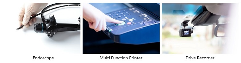
In fact, V-by-One® HS has been used for a variety of applications besides the internal interface of LCD TVs (Figure 1). Figure 1 shows a case where the product is used as a high-speed general-purpose serial interface that communicates data from point A to point B.
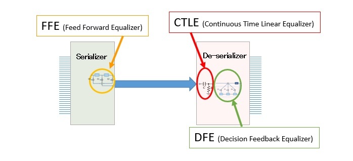
From a technical point of view, V-by-One® HS is simply a SerDes chip. SerDes is a technical term that combines Serializer with Deserializer. The serializer converts parallel signals into serial and then transmits the data by multi signal lines (Figure 2). After that, the deserializer converts the received serial signals back into parallel.

First of all THine Electronics focused on the high resolution LCD and released V-by-One® HS family with high-speed serial interfaces for the application. Then these were also employed to other markets.
V-by-One® HS interface are defined for LCD panel signals such as “R [Red] [0-9], G [Green] [0-9], B [Blue] [0-9]” or “Vsync, Hsync, De”. These are possible to change to general purpose bus signals.
Figure 1 Examples of V-by-One® HS applications
From a technical point of view, V-by-One® HS is simply a SerDes chip. SerDes is a technical term that combines Serializer with Deserializer. The serializer converts parallel signals into serial and then transmits the data by multi signal lines (Figure 2). After that, the deserializer converts the received serial signals back into parallel.

Figure 2 Serializer and De-serializer
First of all THine Electronics focused on the high resolution LCD and released V-by-One® HS family with high-speed serial interfaces for the application. Then these were also employed to other markets.
V-by-One® HS interface are defined for LCD panel signals such as “R [Red] [0-9], G [Green] [0-9], B [Blue] [0-9]” or “Vsync, Hsync, De”. These are possible to change to general purpose bus signals.
Better user experience requires higher data transmission
What is also important that the data rate of the digital interface for LCD TV. With rapid enhancement of the image quality, there has been a sharply growing demand in increasing of the data rate. Specifically, there is simultaneous growth in resolution, high frame rate (HFR), and in high dynamic range (HDR). This situation has resulted in very high demand for higher data rate. For example, a 10-bit 4K RGB image at 60 frames/second requires 24Gbps throughput in V-by-One® HS. This high-speed interface has been achieved by V-by-One® HS with 3Gbps x 8 lanes. However, users are not satisfied with 60 frames/second. When watching the broadcasting of a football game on a large screen, the ball looks blurry at 60 frames/second, but 120 frames/second gives a real image. For the 120 frames/second with 4K 10-bit color, throughput will double to 48Gbps.
What is more, NHK has already begun 8K test broadcasting in Japan. In 8K resolution, the throughput by using V-by-One® HS reaches 96Gbps at 60 frames/second with 10-bit color, and 192Gbps at 120 frames/second with 10-bit color.
What is more, NHK has already begun 8K test broadcasting in Japan. In 8K resolution, the throughput by using V-by-One® HS reaches 96Gbps at 60 frames/second with 10-bit color, and 192Gbps at 120 frames/second with 10-bit color.
Achieved 256Gbps by 16Gbps x 16 lanes
THine Electronics has already established solutions for 8K at 120 frames/second. This solution is V-by-One® US, the next generation of V-by-One® HS. The maximum data rate is 16Gbps per lane, which is four times faster than V-by-One® HS. The 8K 12-bit color. with 120 frames/second is used V-by-One® US 14.85Gbps with 16 lanes.
This fact means that THine Electronics has the technology of the general purpose high speed interface up to 16Gbps with multi lanes already. This high speed technology will apply to interfaces for high rate data transmission between point A and point B as well as to the digital interfaces LCD TV.
This fact means that THine Electronics has the technology of the general purpose high speed interface up to 16Gbps with multi lanes already. This high speed technology will apply to interfaces for high rate data transmission between point A and point B as well as to the digital interfaces LCD TV.
Physical layer technology for high data rate: FFE, CTLE, DFE
What physical layer technology is used for V-by-One® US to achieve the high data rate? Basically, the multiple signal conditioning technique are applied, which is commonly used for SerDes and re-timer IC (CDR) for data communication applications for 10 to 32Gbps.
FFE (Feed-Forward Equalizer) is used for a transmitter, and DFE (Decision Feedback Equalizer) and CTLE (Continuous Time Linear Equalizer) are used for the receiver (Figure 3).
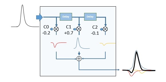
Here is a brief description of each technologies. The built-in FFE in a transmitter is a technology having multi-tap de-emphasis and pre-emphasis functions which enables more flexible waveform adjustment. Specifically, the FFE provides a tap consisting of multiple delay blocks and adds up signals amplified or attenuated at a given ratio in the individual delay blocks and then outputs the added value (Figure 4).
This allows expected transmission waveform to be created for the (pre- and de-) emphasis and pre-shooting of the waveform for a receiver which requires a clean Eye.
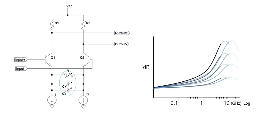
The CTLE (Continuous Time Linear Equalizer) in a receiver is an analog technology which amplifies and compensates high frequency insertion loss for transmission line (Figure 5). This means that it functions as a high-pass filter and amplifier.
The other technology for a receiver, DFE (Decision Feedback Equalizer), reduces the ISI (Inter Symbol Interference) jitter of received signals. As like FFE, DFE consists of multiple taps. The DFE determines the tap coefficient for each 1 UI so that the error between a received waveform and an ideal waveform can be minimized and then gives feedback for the received signal waveform (Figure 6). This behavior reduces jitter and returns the signal waveform with a clean Eye opening.
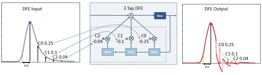
The role sharing of the CTLE and DFE for signal waveforms with completely closed Eye is as follows: first, the CTLE is applied to open Eye roughly, and then the DFE reduce jitter more for clean Eye.
FFE (Feed-Forward Equalizer) is used for a transmitter, and DFE (Decision Feedback Equalizer) and CTLE (Continuous Time Linear Equalizer) are used for the receiver (Figure 3).
Figure 3 Application of FFE to the transmitter and CTLE and DFE to the receiver
Here is a brief description of each technologies. The built-in FFE in a transmitter is a technology having multi-tap de-emphasis and pre-emphasis functions which enables more flexible waveform adjustment. Specifically, the FFE provides a tap consisting of multiple delay blocks and adds up signals amplified or attenuated at a given ratio in the individual delay blocks and then outputs the added value (Figure 4).
Figure 4 Mechanism of FFE (Feed Forward Equalizer)
This allows expected transmission waveform to be created for the (pre- and de-) emphasis and pre-shooting of the waveform for a receiver which requires a clean Eye.
The CTLE (Continuous Time Linear Equalizer) in a receiver is an analog technology which amplifies and compensates high frequency insertion loss for transmission line (Figure 5). This means that it functions as a high-pass filter and amplifier.
Figure 5 Mechanism of CTLE (Continuous Time Linear Equalizer)
The other technology for a receiver, DFE (Decision Feedback Equalizer), reduces the ISI (Inter Symbol Interference) jitter of received signals. As like FFE, DFE consists of multiple taps. The DFE determines the tap coefficient for each 1 UI so that the error between a received waveform and an ideal waveform can be minimized and then gives feedback for the received signal waveform (Figure 6). This behavior reduces jitter and returns the signal waveform with a clean Eye opening.
Figure 6 Mechanism of DFE (Decision Feedback Equalizer)
The role sharing of the CTLE and DFE for signal waveforms with completely closed Eye is as follows: first, the CTLE is applied to open Eye roughly, and then the DFE reduce jitter more for clean Eye.
Development of the V-by-One® US transmission media in collaboration with FFC/connector manufacturers
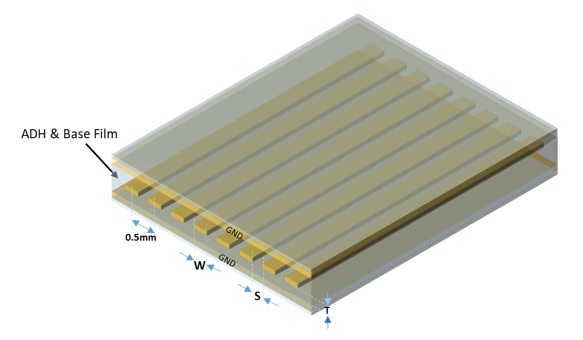
In addition, THine Electronics has not only developed the chip for V-by-One® US but has also been collaborating with FFC/connector manufacturers to develop a flexible flat cable (FFC) and connector for the transmission line of a high speed digital interface. THine achieved the high-speed inter-connect technology for the high-speed media with 16Gbps x 16 lanes by a long-reach FFC up to 1m.
This broadband low-loss FFC optimizes its materials and structure. Materials having small dielectric loss tangent (tanδ) and dielectric constant (εr) are used to reduce propagation loss. In addition, an optimized layout minimizes the transmission media loss, reflection loss, and cross-talk (Figure 7). While keeping the current structure of the FFC receptacle connector, an impedance is adjusted by improving the structure and metal part of the solder connection of connector pins and wiring on a substrate and/or by changing the wiring length in order to reduce signal reflection.
There will be some issues for high speed 16Gbps x 16 lanes interface. It is a signal path of V-by-One® US chip, a printed circuit board line, and connectors. Because this is the work to be done by users. THine Electronic says, “PCB art-work should be carefully made because the materials and layer structure of a print circuit board significant affect the electric characteristics, and it is important to manage the impedance control at the connecting point with each components.”
This broadband low-loss FFC optimizes its materials and structure. Materials having small dielectric loss tangent (tanδ) and dielectric constant (εr) are used to reduce propagation loss. In addition, an optimized layout minimizes the transmission media loss, reflection loss, and cross-talk (Figure 7). While keeping the current structure of the FFC receptacle connector, an impedance is adjusted by improving the structure and metal part of the solder connection of connector pins and wiring on a substrate and/or by changing the wiring length in order to reduce signal reflection.
Figure 7 Basic structure of FFC for 16 Gbps (double-sided shield type)
There will be some issues for high speed 16Gbps x 16 lanes interface. It is a signal path of V-by-One® US chip, a printed circuit board line, and connectors. Because this is the work to be done by users. THine Electronic says, “PCB art-work should be carefully made because the materials and layer structure of a print circuit board significant affect the electric characteristics, and it is important to manage the impedance control at the connecting point with each components.”
The development of next-generation
THine Electronics focus next-generation solution with a higher data rate than V-by-One® US. By expanding lineup of high-speed interfaces family, THine intends to solidify its corporate brand equity as “THine known for its high-speed interfaces.”
By releasing the high-speed products, the company shows to have the advanced technology and brand equity.
The other reason is that there is a big market which requires the technology. There needs higher data rate in communication infrastructure and data center markets. In the communication infrastructure market, there are needs for communication of picture images with control data without delay in response to demands for 5G. In the data center market, AI/GPU requires high processing performance, hence it uses high-speed communication.
The next generation high speed interface products will change the corporate brand equity from “THine best known for its LCD TV” to “THine best known for its high-speed interfaces."
Related Contents
- V-by-One® HS goes beyond LVDS, making its presence known in medical, automotive and various other applications
- V-by-One® HS goes beyond LVDS -Long distance transmission at a high speed is achieved with high reliable 8B/10B coding and signal conditioning technology-
- Deep dive about the Basic Principle of LVDS SerDes, Taking advantage of its features – high speed, long distance, low noise
- History of THine products for signal transmission started from SerDes IC for laptop PC