THine Value Deep dive about the Basic Principle of LVDS SerDes, Taking advantage of its features – high speed, long distance, low noise
2017.10.10
- Article
- Column
A serial interface connects devices such as between a liquid crystal panel and a logic board. In the first installment of this series, looking back at its history, we introduced the advancement of its technology, our efforts to improve performance, and changes in use in applications. Now, we will explain in detail about the basic principle, features, and available products, with focus on the technology of LVDS (low voltage differential signaling).
Supported the PC market for more than 15 years
It is no exaggeration to say that LVDS technology opened the history of the serial interface. In the mid-1990s, the technology was adopted in laptop PCs, the market of which was rapidly expanding, resulting in a dramatic increase in the shipment volume of LVDS SerDes. There is no doubt about the fact that LVDS played a great role in spreading laptop PCs worldwide and made a great contribution to the emergence of the LCD (Liquid Crystal Display) market.
LVDS SerDes for laptop PCs were later integrated in chip sets for PCs and/or liquid crystal timing controller IC (TCON). It also became compatible with the liquid crystal panels with a high resolution such as UXGA and WUXGA. This made LVDS SerDes continue to be used for more than 15 years. Although it has been gradually replaced by eDP (embedded DisplayPort) for laptop PCs since around 2012, it has supported the laptop PC market until recently.
Having said so, LVDS SerDes is not an exclusive interface technology for connecting between a liquid crystal panel and a logic board. If you look at what its technology is, it is quite obvious that LVDS SerDes is a general serial interface technology connecting an A point and a B point. Therefore, it can be used for interfacing in various applications. Then, how or in what applications can we use it to bring out its best performance? We will answer this question below.
Used for high-speed data transmission
To use LVDS SerDes fully, it is necessary, to understand the technology of the LVDS, which has been specified as a physical layer.
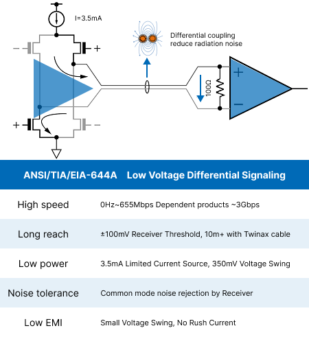
LVDS, which was standardized as ANSI/TIA/EIA-644A in 1995, is a physical layer specification for serial interface (Fig.1). It is activated by the 3.5mA constant current, and transmits high speed differential signal data with a very low voltage swing of 350mV terminated with a 100Ω load. The data transmission speed is designated by the Standard as 655M bits/sec at the maximum. But it is not the limit. Semiconductor manufacturers, incorporating their own technology, have achieved higher data transmission speed up to around 3G bits/sec.
Fig. 2 shows a specific example of the differential signal waveform of LVDS.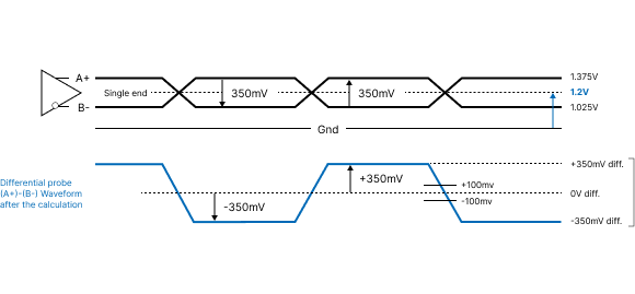
Two differential signals, positive signal (A+) and negative signal (B-), are swung with a 1.2V common-mode voltage (Voc) in the middle. There is a potential difference of 350mV between the two signals. If measured by a differential probe connected to an oscilloscope, the signal waveform like Fig. 2 is obtained. It shows a difference of voltage swing of the two signals ([A+] – [B-]). Measurement with a differential probe displays the result of the calculation of voltage swing difference, but it does not mean that the signal waveform exists like this physically.
The range of Voc of an LVDS receiver is shown in Fig. 3.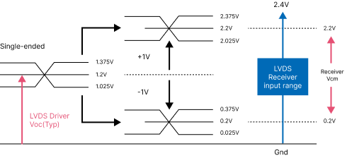
As evidenced by Fig. 3, an LVDS receiver has a wide range of Voc to receive data. Although the transmitter side outputs data with a Voc of 1.2V, the receiver side can receive data if the range of Voc is from 0.2V to 2.2V.
Furthermore, since LVDS SerDes transmits data in the form of differential signals with a low voltage swing, electro-magnetic interference (EMI) noise radiation can be suppressed. This prevents EMI noise from affecting other circuits and causing negative influence. This is one of the reasons why LVDS SerDes is adopted in electronic equipment that is sensitive to signal noise.
To sum up, the advantages of LVDS SerDes are its ability to transmit data at a high speed over a long distance, its high Common mode voltage tolerance, and low EMI noise. Its most appropriate application can be electronic equipment that requires these advantages. A good example is a multifunction printer (MFP).
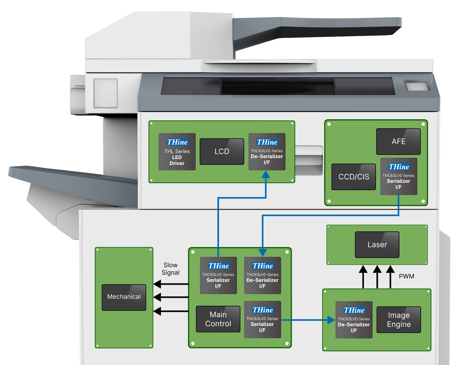
In the MFP, not only being used to interface with the liquid crystal display panel, LVDS SerDes is also used to send image data obtained by the scanner (image sensor) to the main board that carries out image processing. Devices are placed rather far away from each other inside the printer (Fig.4). LVDS SerDes allows a scanner and a main board to be located far away, because it is able to transmit data for a few meters with a thin cable without problem although it depends on the skew of the cable in use or the magnitude of power loss. LVDS SerDes is one of the most suitable solutions for the internal (inside-the-box) high-speed data transmission.

Fig. 1 Specification of LVDS (Low Voltage Differential Signaling)
LVDS, which was standardized as ANSI/TIA/EIA-644A in 1995, is a physical layer specification for serial interface (Fig.1). It is activated by the 3.5mA constant current, and transmits high speed differential signal data with a very low voltage swing of 350mV terminated with a 100Ω load. The data transmission speed is designated by the Standard as 655M bits/sec at the maximum. But it is not the limit. Semiconductor manufacturers, incorporating their own technology, have achieved higher data transmission speed up to around 3G bits/sec.
Fig. 2 shows a specific example of the differential signal waveform of LVDS.

Fig. 2 LVDS differential signals (single end and differential)
Two differential signals, positive signal (A+) and negative signal (B-), are swung with a 1.2V common-mode voltage (Voc) in the middle. There is a potential difference of 350mV between the two signals. If measured by a differential probe connected to an oscilloscope, the signal waveform like Fig. 2 is obtained. It shows a difference of voltage swing of the two signals ([A+] – [B-]). Measurement with a differential probe displays the result of the calculation of voltage swing difference, but it does not mean that the signal waveform exists like this physically.
The range of Voc of an LVDS receiver is shown in Fig. 3.

Fig. 3 Common-mode voltage of an LVDS receiver
As evidenced by Fig. 3, an LVDS receiver has a wide range of Voc to receive data. Although the transmitter side outputs data with a Voc of 1.2V, the receiver side can receive data if the range of Voc is from 0.2V to 2.2V.
Furthermore, since LVDS SerDes transmits data in the form of differential signals with a low voltage swing, electro-magnetic interference (EMI) noise radiation can be suppressed. This prevents EMI noise from affecting other circuits and causing negative influence. This is one of the reasons why LVDS SerDes is adopted in electronic equipment that is sensitive to signal noise.
To sum up, the advantages of LVDS SerDes are its ability to transmit data at a high speed over a long distance, its high Common mode voltage tolerance, and low EMI noise. Its most appropriate application can be electronic equipment that requires these advantages. A good example is a multifunction printer (MFP).
In the MFP, not only being used to interface with the liquid crystal display panel, LVDS SerDes is also used to send image data obtained by the scanner (image sensor) to the main board that carries out image processing. Devices are placed rather far away from each other inside the printer (Fig.4). LVDS SerDes allows a scanner and a main board to be located far away, because it is able to transmit data for a few meters with a thin cable without problem although it depends on the skew of the cable in use or the magnitude of power loss. LVDS SerDes is one of the most suitable solutions for the internal (inside-the-box) high-speed data transmission.
Robust against signal skew and common-mode voltage
Currently, various LVDS SerDes products are available. Here is an introduction of actual products using product families from THine as examples.
Fig. 5 illustrates the basic configuration of LVDS SerDes.
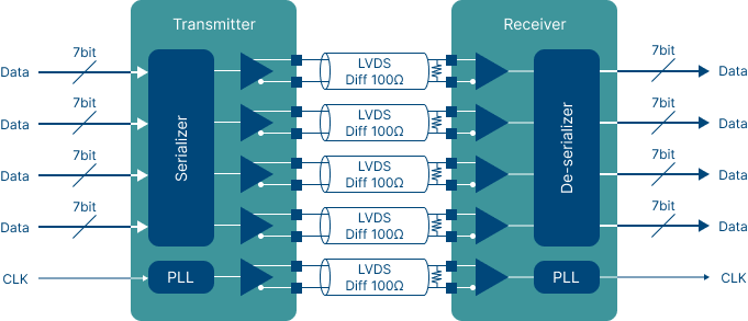
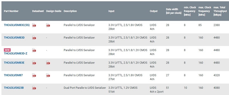
Incoming signals to the serializer are four 7-bit data streams, i.e., 28 bits of data. These data are converted into serial LVDS signals and sent to the deserializer. Clock signals are sent separately. The deserializer, using the clock signals it receives, adjusts the timing of receiving data, and converts the four 7-bit LVDS data streams into TTL/CMOS data, which are output. This is the mechanism of LVDS SerDes. THine offers LVDS SerDes products as listed in the Table 1, and they have six features, which will be explained below.
The first feature is that, in addition to the general products that activate at 3.3V, THine provides products that activate at a low voltage of 1.8V while meeting the LVDS Standard. Typically, if the source voltage is low, it becomes difficult to maintain 1.2V of common-mode output voltage (Voc), which is stipulated in the LVDS Standard. There are few low-voltage-activated products with the Voc falling below 1.2V. However, THine “THC63LVDM87” and “THC63LVD827” achieve low-voltage activation at 1.8V, and at the same time, maintain Voc at 1.2V, the most suitable power level for the deserializer on the receiver side.
The second feature is that THine’s lineup includes various single-link and dual-link products. For example, “THC63LVD103D” is a single-link serializer used for transmission of 10–bit RGB image signal, and its dual-link version is “THC63LVD1023B.” In the same way, “THC63LVD104C” is a single-link deserializer and its dual-link version is “THC63LVD1024.” If you use a dual-link product, you can easily expand the data transmission band. For example, single-link products accommodate only up to 1080i, but dual-link products handle1080p. Furthermore, 8-bit RGB dual-link products are available, specifically, serializer “THC63LVD823B” and deserializer “THC63LVD824A.”
Thirdly, users are allowed to select THine’s products according to the timing of data acquisition, i.e., the rising edge or falling edge. For liquid crystal panels, the falling edge is used, while for the serial interface for general data transmission, the rising edge is used. If a part number has “R” as in “LVDR,” the product acquires rising edge data. If “LVDF” is found in the part number, the product acquires falling edge data. If a part number has “LVDM” or “LVD,” it works for both and you can select either by setting a pin.
Fourthly, a repeater IC is also commercialized with the part number “THC63LVD1027.” The repeater IC receives signals output from LVDS Serializer, absorbs skew and jitter generated in the long cable, and sends LVDS signals in an ideally adjusted condition both in terms of voltage and timing (Fig.6).
With the help of the repeater IC, the data transmission distance (cable length) can be significantly extended. If the repeater IC is placed midway in the transmission path, the data transmission distance (cable length) can be doubled. In addition, the repeater IC can divide single-channel incoming image signals into two channels for output (Fig. 7). Before this product, it was very difficult to divide LVDS SerDes signals.
The fifth feature of THine’s products is the wide range of clock frequency, namely 8-160MHz. “THC63LVD103D” is one of such products. With a wide range of clock frequency, the product can be used for various parallel buses, allowing for more flexible design.
The sixth feature is lower voltage swing in some of THine’s products. As aforementioned, typical LVDS SerDes uses a current source of 3.5mA and a 100Ω termination resistor, making the voltage swing 350mV. But if an RS (reduce swing) in the LVDS low voltage swing mode is used, the voltage swing can be reduced to 200mV, making it possible to suppress EMI and reduce power consumption.
The other feature is THine’s unique lineup that covers:
- A product which has a 49-pin VFBGA 5mm x 5mm small package for small electronic devices such as a camera module.
- Products that work in a wide range of temperature, from -40℃ to +105℃, to be used in industrial as well as automotive related application.
As described above, THine provides many LVDS SerDes products, offering a wide range of capabilities for a variety of applications. However, all serial interfaces cannot be covered by LVDS SerDes alone. LVDS SerDes is difficult to use in applications that require both high speed and long transmission distance, or high-resolution signals such as 4X speed, deep colors, and 8K. To solve this, THine offers “V-by-One® HS,” an even higher-speed serial interface technology. In the next installment, we will explain the basic principle of “V-by-One® HS” and THine’s variety of products based on it.
Fig. 5 illustrates the basic configuration of LVDS SerDes.

Fig. 5 LVDS SerDes for 28 bits of data
Incoming signals to the serializer are four 7-bit data streams, i.e., 28 bits of data. These data are converted into serial LVDS signals and sent to the deserializer. Clock signals are sent separately. The deserializer, using the clock signals it receives, adjusts the timing of receiving data, and converts the four 7-bit LVDS data streams into TTL/CMOS data, which are output. This is the mechanism of LVDS SerDes. THine offers LVDS SerDes products as listed in the Table 1, and they have six features, which will be explained below.
Table 1 List of LVDS SerDes products
The first feature is that, in addition to the general products that activate at 3.3V, THine provides products that activate at a low voltage of 1.8V while meeting the LVDS Standard. Typically, if the source voltage is low, it becomes difficult to maintain 1.2V of common-mode output voltage (Voc), which is stipulated in the LVDS Standard. There are few low-voltage-activated products with the Voc falling below 1.2V. However, THine “THC63LVDM87” and “THC63LVD827” achieve low-voltage activation at 1.8V, and at the same time, maintain Voc at 1.2V, the most suitable power level for the deserializer on the receiver side.
The second feature is that THine’s lineup includes various single-link and dual-link products. For example, “THC63LVD103D” is a single-link serializer used for transmission of 10–bit RGB image signal, and its dual-link version is “THC63LVD1023B.” In the same way, “THC63LVD104C” is a single-link deserializer and its dual-link version is “THC63LVD1024.” If you use a dual-link product, you can easily expand the data transmission band. For example, single-link products accommodate only up to 1080i, but dual-link products handle1080p. Furthermore, 8-bit RGB dual-link products are available, specifically, serializer “THC63LVD823B” and deserializer “THC63LVD824A.”
Thirdly, users are allowed to select THine’s products according to the timing of data acquisition, i.e., the rising edge or falling edge. For liquid crystal panels, the falling edge is used, while for the serial interface for general data transmission, the rising edge is used. If a part number has “R” as in “LVDR,” the product acquires rising edge data. If “LVDF” is found in the part number, the product acquires falling edge data. If a part number has “LVDM” or “LVD,” it works for both and you can select either by setting a pin.
Fourthly, a repeater IC is also commercialized with the part number “THC63LVD1027.” The repeater IC receives signals output from LVDS Serializer, absorbs skew and jitter generated in the long cable, and sends LVDS signals in an ideally adjusted condition both in terms of voltage and timing (Fig.6).

Fig. 6 A use example of LVDS repeater IC (1)
With the help of the repeater IC, the data transmission distance (cable length) can be significantly extended. If the repeater IC is placed midway in the transmission path, the data transmission distance (cable length) can be doubled. In addition, the repeater IC can divide single-channel incoming image signals into two channels for output (Fig. 7). Before this product, it was very difficult to divide LVDS SerDes signals.

Fig. 7 A use example of LVDS repeater IC (2)
The fifth feature of THine’s products is the wide range of clock frequency, namely 8-160MHz. “THC63LVD103D” is one of such products. With a wide range of clock frequency, the product can be used for various parallel buses, allowing for more flexible design.
The sixth feature is lower voltage swing in some of THine’s products. As aforementioned, typical LVDS SerDes uses a current source of 3.5mA and a 100Ω termination resistor, making the voltage swing 350mV. But if an RS (reduce swing) in the LVDS low voltage swing mode is used, the voltage swing can be reduced to 200mV, making it possible to suppress EMI and reduce power consumption.
The other feature is THine’s unique lineup that covers:
- A product which has a 49-pin VFBGA 5mm x 5mm small package for small electronic devices such as a camera module.
- Products that work in a wide range of temperature, from -40℃ to +105℃, to be used in industrial as well as automotive related application.
As described above, THine provides many LVDS SerDes products, offering a wide range of capabilities for a variety of applications. However, all serial interfaces cannot be covered by LVDS SerDes alone. LVDS SerDes is difficult to use in applications that require both high speed and long transmission distance, or high-resolution signals such as 4X speed, deep colors, and 8K. To solve this, THine offers “V-by-One® HS,” an even higher-speed serial interface technology. In the next installment, we will explain the basic principle of “V-by-One® HS” and THine’s variety of products based on it.
*Note:
Fig. 6: A use example of LVDS repeater IC (1)
A use example of “THC63LVD1027,” an LVDS SerDes dual-channel repeater IC. It is placed in the transmission path to extend the transmission distance.
Fig. 7: A use example of LVDS repeater IC (2)
A use example of “THC63LVD1027,” an LVDS SerDes dual-channel repeater IC. It can be used for 1:2 signal distribution – dividing single-channel incoming image signals into two channels for output.
Related Contents
- The technology of V-by-One® SerDes apply not only to TV application but to high-speed interfaces for communication/computer/industrial equipment as well
- V-by-One® HS goes beyond LVDS, making its presence known in medical, automotive and various other applications
- V-by-One® HS goes beyond LVDS -Long distance transmission at a high speed is achieved with high reliable 8B/10B coding and signal conditioning technology-
- History of THine products for signal transmission started from SerDes IC for laptop PC

