![]()
THine Value Higher Refresh Rates and Lower Power Consumption for TVs! Introducing the V-by-One HS plus Standard
2023.07.11
- Article
- Column
A video interface connects a video processor (video processing SoC) and a timing controller (TCON) inside the TV. THine Electronics provides transmitter/receiver ICs for this type of video interface, as well as a technical standard used by such interfaces, which the TV industry has widely adopted. We call this standard/technology V-by-One HS.
V-by-One HS began wide adoption in the industry around 2011. The standard has been in use ever since, for twelve years. For this reason, many in the TV industry call V-by-One HS the de facto standard for video interfaces.
Recently, there has been a change in the trends around this type of video interface. There are two trends to discuss. One is the aim to further improve TV image quality. Specifically, this includes a higher resolution and higher refresh rate. The definition of "high resolution" is shifting from 4K (approx. 4,000 by 2,000 pixels) to 8K (approx. 8,000 by 4,000 pixels). The trend toward higher refresh rates is to increase the current mainstream of 120 Hz to 165 Hz or 240 Hz. One of the reasons behind this trend toward higher refresh rates is the consideration of equipping TVs with a gaming mode, which is effective for playing games that require real-time performance, such as esports. Gaming monitors, or PC monitors that support high refresh rates, already exist in the market. The intention is to enable TVs to compete with their real-time performance. This function also attracts attention from the perspective of adding value to TV sets, which have become remarkably commoditized in recent years.
The other of the two trends is further low power consumption. The trend toward stricter environmental regulations for consumer electronics, particularly in Europe and the U.S., has led to a strong demand for reduced power consumption in electronic devices. Of course, TV sets are no exception. For this reason, TV manufacturers are working to reduce the power consumption of each element that makes up a TV. This lower power consumption is expected, in full, for video interfaces as well. TV manufacturers continue to face a difficult situation in which they must strive for higher performance while at the same time reducing power consumption.
Transmission Rate up to 8 Gbps
The two trends in recent TVs are higher video quality and lower power consumption. As a provider of V-by-One HS, which is widely used as a video interface inside TVs, THine Electronics sees it as one of its responsibilities to address these two trends.
In response, THine Electronics has formulated a new interface standard, V-by-One HS plus, as the successor to V-by-One HS (Fig. 1).
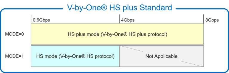
Licensing for this standard began on June 1, 2023. Although the existing V-by-One HS will remain available, new licensing of the V-by-One HS standard will be sunsetted. Afterward, the V-by-One HS standard will be integrated into the V-by-One HS plus standard. The V-by-One HS plus defines two modes: "HS mode," fully compatible with the last version of V-by-One HS, Ver. 1.52, and "HS plus mode," newly added in V-by-One HS plus. Users can implement either of these modes or both at the same time (Fig. 2).
The most significant feature of the HS plus mode is that the maximum data transmission rate (bandwidth) has been increased to 8 Gbps. Conventional V-by-One HS speeds topped at 4 Gbps, meaning the HS plus mode doubles in speed. High speed is achieved by doubling the clock frequency of the transmission signal.
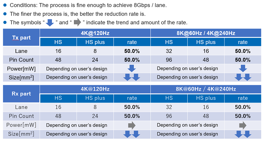
This will enable TV manufacturers to meet the demand for higher video quality and lower power consumption. A specific example is given below, assuming a TV set with a resolution of 4K and a refresh rate of 120 Hz. For the purpose of improving video quality, HS plus mode can be applied to a TV with 120 Hz at 4K resolution to upgrade the TV to one with 60 Hz at 8K resolution or 240 Hz at 4K resolution, while keeping the exact same number of signal line lanes connecting the video processor and TCON.
On the other hand, if HS plus mode is applied to a 120 Hz TV with 4K resolution for lower power consumption, the number of lanes connecting the video processor and TCON can be reduced by half while maintaining the same resolution and refresh rate. A reduced number of lines will likely reduce the power consumption of the video processor, especially on the transmitter side (Fig. 3 and Fig. 4). Thus, the HS plus mode opens up the possibility for higher video quality and lower power consumption.
.png?v=1708481493)
In response, THine Electronics has formulated a new interface standard, V-by-One HS plus, as the successor to V-by-One HS (Fig. 1).
Fig. 1 V-by-One HS plus logo
Licensing for this standard began on June 1, 2023. Although the existing V-by-One HS will remain available, new licensing of the V-by-One HS standard will be sunsetted. Afterward, the V-by-One HS standard will be integrated into the V-by-One HS plus standard. The V-by-One HS plus defines two modes: "HS mode," fully compatible with the last version of V-by-One HS, Ver. 1.52, and "HS plus mode," newly added in V-by-One HS plus. Users can implement either of these modes or both at the same time (Fig. 2).
Fig. 2 Definition of each mode in the V-by-One HS plus standard
The most significant feature of the HS plus mode is that the maximum data transmission rate (bandwidth) has been increased to 8 Gbps. Conventional V-by-One HS speeds topped at 4 Gbps, meaning the HS plus mode doubles in speed. High speed is achieved by doubling the clock frequency of the transmission signal.
This will enable TV manufacturers to meet the demand for higher video quality and lower power consumption. A specific example is given below, assuming a TV set with a resolution of 4K and a refresh rate of 120 Hz. For the purpose of improving video quality, HS plus mode can be applied to a TV with 120 Hz at 4K resolution to upgrade the TV to one with 60 Hz at 8K resolution or 240 Hz at 4K resolution, while keeping the exact same number of signal line lanes connecting the video processor and TCON.
On the other hand, if HS plus mode is applied to a 120 Hz TV with 4K resolution for lower power consumption, the number of lanes connecting the video processor and TCON can be reduced by half while maintaining the same resolution and refresh rate. A reduced number of lines will likely reduce the power consumption of the video processor, especially on the transmitter side (Fig. 3 and Fig. 4). Thus, the HS plus mode opens up the possibility for higher video quality and lower power consumption.
Fig. 3 Number of lanes reduced by half
Fig. 4 Variation of each element when V-by-One HS plus is applied
System Cost Advantages with V-by-One HS plus
All manufacturers face the need for higher video quality and lower power consumption. However, cost reduction is an equally important issue. To this end, we will review the cost factors involved in V-by-One HS plus from two perspectives: the cost of components related to the configuration of the video interface and the cost of licensing the V-by-One HS plus standard.
Our first task is to review the cost of related components for the video interface. In HS plus mode, the maximum data transmission speed has been increased to 8 Gbps, twice the speed of the conventional standard, but the basic signal transmission method has changed little from the HS mode (Fig. 5).
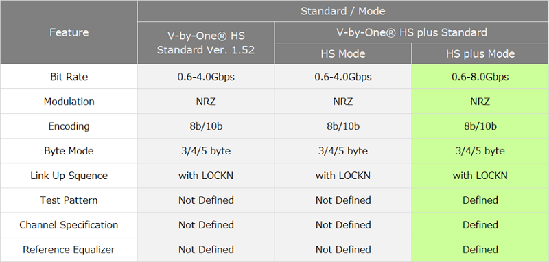
For example, the modulation and encoding methods are exactly the same. This means that in addition to TV manufacturers, LSI manufacturers developing video processors and TCONs can use many of the design assets and manufacturing environments developed for the V-by-One HS generation for V-by-One HS plus. This cross-platform use will reduce the cost of technical migration to a new interface and the initial development cost. For connectors and cables, which significantly impact cost factors, the same ones as those used for the conventional V-by-One HS can be used. The technical components that support the establishment of high-speed transmission, which has been increased to 8 Gbps for V-by-One HS plus, include the "Reference Equalizer," which was newly defined in V-by-One HS plus, the "Test Pattern," connection test specification, and the "Channel Specification" that defines the characteristics of the signal transmission path.
Another component that should not be overlooked is the cost of video processors and TCONs that incorporate circuitry compliant with the interface standard. The decrease in transmission paths with higher speeds contributes to a reduction in the number of input/output pins of the transmitter (video processor) and receiver (TCON) LSIs, package dimensions, and die size inside the package, which in turn leads to a reduction in overall LSI cost (see Fig. 4 for each reduction factor in LSI cost).
Our first task is to review the cost of related components for the video interface. In HS plus mode, the maximum data transmission speed has been increased to 8 Gbps, twice the speed of the conventional standard, but the basic signal transmission method has changed little from the HS mode (Fig. 5).
Fig. 5 Comparison of key specifications of V-by-One HS plus and V-by-One HS standards
For example, the modulation and encoding methods are exactly the same. This means that in addition to TV manufacturers, LSI manufacturers developing video processors and TCONs can use many of the design assets and manufacturing environments developed for the V-by-One HS generation for V-by-One HS plus. This cross-platform use will reduce the cost of technical migration to a new interface and the initial development cost. For connectors and cables, which significantly impact cost factors, the same ones as those used for the conventional V-by-One HS can be used. The technical components that support the establishment of high-speed transmission, which has been increased to 8 Gbps for V-by-One HS plus, include the "Reference Equalizer," which was newly defined in V-by-One HS plus, the "Test Pattern," connection test specification, and the "Channel Specification" that defines the characteristics of the signal transmission path.
Another component that should not be overlooked is the cost of video processors and TCONs that incorporate circuitry compliant with the interface standard. The decrease in transmission paths with higher speeds contributes to a reduction in the number of input/output pins of the transmitter (video processor) and receiver (TCON) LSIs, package dimensions, and die size inside the package, which in turn leads to a reduction in overall LSI cost (see Fig. 4 for each reduction factor in LSI cost).
Types of Licenses for V-by-One HS plus
Next, the licensing costs for the V-by-One HS plus are described. The new standard defines each license type as shown in Fig. 6. It is assumed that paid licenses will be granted to users who design LSIs and IP cores (LSI manufacturers and IP core vendors) and to users who design FPGAs using IP cores.
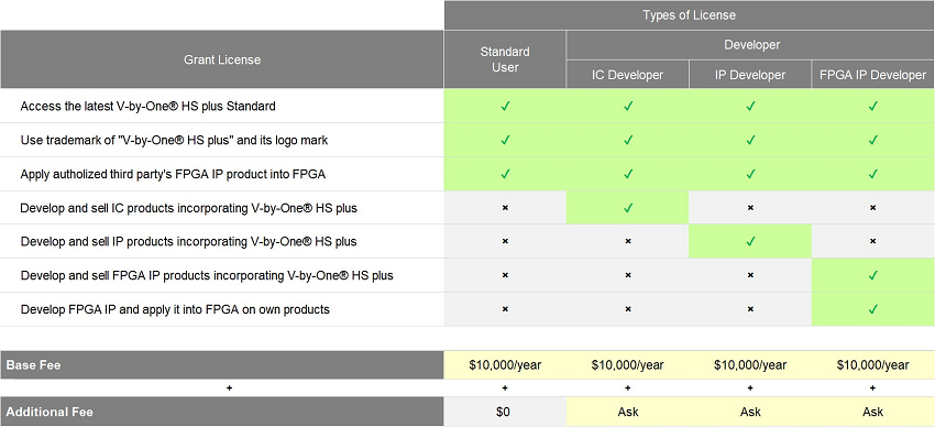
One change from the past is that users who do not design LSIs, IP cores, or FPGAs but only wish to obtain the standard (license for the right to view the standard) are now required to obtain a paid license as a "Standard User." If using V-by-One HS/HS plus compliant ICs sold by THine Electronics or V-by-One HS/HS plus compliant ICs provided by licensees licensed by THine Electronics, no license fee will be charged as in the past.
With the change in license types from the existing V-by-One HS standard, the direct and indirect license costs incurred by V-by-One HS plus may become relatively large. However, THine Electronics believes that V-by-One HS plus will contribute to the success of each licensee, given the factors mentioned above that reduce the cost of various components and add value to the end product.
Fig. 6 License types for the V-by-One HS plus standard
One change from the past is that users who do not design LSIs, IP cores, or FPGAs but only wish to obtain the standard (license for the right to view the standard) are now required to obtain a paid license as a "Standard User." If using V-by-One HS/HS plus compliant ICs sold by THine Electronics or V-by-One HS/HS plus compliant ICs provided by licensees licensed by THine Electronics, no license fee will be charged as in the past.
With the change in license types from the existing V-by-One HS standard, the direct and indirect license costs incurred by V-by-One HS plus may become relatively large. However, THine Electronics believes that V-by-One HS plus will contribute to the success of each licensee, given the factors mentioned above that reduce the cost of various components and add value to the end product.
An Outlook of Faster Speeds and Lower Power Consumption
Although we have just formulated the V-by-One HS plus standard, THine Electronics has already drawn up a blueprint for extending the specification. At this time, there are two specification extensions under consideration.
One of these extensions is to provide an even higher increase in speed. The current maximum data transmission speed is 8 Gbps, but analyses are underway to speed this up one more step to 9 Gbps. The difference between 8 Gbps and 9 Gbps may initially seem small, but the technical barrier in this 1 Gbps is not insignificant at this stage. However, once technical feasibility is achieved, speeds can be increased to 9 Gbps to lower to expand applications that may reduce the number of lanes.
The other of these extensions is to introduce a low-power consumption mode. The refresh rate of a TV is not always required to be at its maximum value. For example, if the media is updated rather infrequently, such as when displaying thumbnails for a video streaming service, the effect of lowering the refresh rate may be small. In this case, the number of signal transmission lanes used can be reduced, and the number of transmitter circuits in operation can be reduced. In other words, power consumption can be reduced when using low-power mode. Since environmental regulations from industry associations are expected to continue to become more stringent in the future, we will continue to consider this type of low-power mode as a way to help address these environmental concerns.
Evaluation Boards for Trial Installation and Verification to the Market
In addition, THine Electronics plans to release evaluation boards and evaluation chips (TEG chips) for applications such as verifying the signal transmission characteristics of V-by-One HS plus. First, in Q4 of 2023, the Company plans to introduce THEVAHSP, an 8 Gbps evaluation board using FPGAs with transmitter and receiver circuits compliant with the V-by-One HS plus standard. Subsequently, in Q2 of 2024, the Company will release the THEVA423/424-V1, an 8 Gbps evaluation board that uses an evaluation chip (TEG chip) compliant with the V-by-One HS plus standard.
Furthermore, the Company is looking to commercialize a transmitter IC (serializer IC) THCV425 and a receiver IC (deserializer IC) THCV426, with a maximum data transmission speed of 9 Gbps. The product release date will depend on the timing of the specification extension of the V-by-One HS plus standard, but it is currently scheduled for Q4 of 2024.
End