![]()
THine Value V-by-One® HS goes beyond LVDS, making its presence known in medical, automotive and various other applications
2018.02.21
- Article
- Column
V-by-One® HS has become the de facto standard in high-speed interface technology as almost all LCD TVs now adopt it for image/video transmission. In addition to LCD TVs, various applications are also using V-by-One® HS.
8B/10B coding robustness
Many applications leverage V-by-One® HS for high-speed data transmission due to its high data rate (4 Gbps) and high robustness.
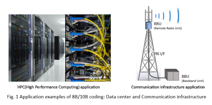
The 8B/10B coding technology was originally developed in the 1980s and then later developed as “InfiniBand” in the 1990s for high performance computing (HPC), the Common Public Radio Interface (CPRI), and the Open Base Station Architecture Initiative (OBSAI) optical interface for communication infrastructure, which accepts no error (Fig. 1).

8B/10B coding provides high robustness. Why?
One reason is that conversion from 8 bits to 10 bits for the 8B10B code map can attenuate 20% of the low-frequency components. This is very effective for reducing inter-symbol interference (ISI) jitter, given the relationship between high-voltage/low-frequency components and attenuated low-voltage/high-frequency components. This enhances signal integrity by reducing ISI jitter when the data rate exceeds the Giga-bit level and where a long cable results in large signal attenuation.
The other reason is that 8B/10B coding secures almost complete DC balance for good signal integrity in AC coupling. This solves problems related to DC balance for data coding (e.g. baseline wander, DC imbalance, killer packet, pathological pattern).
In 8B/10B coding, 8-bit input data are divided into 3 upper bits and 5 lower bits. The 3 bits are converted into 4 bits (3B/4B coding), while the 5 bits are converted into 6 bits (5B/6B coding). The data is converted into a symbol according to a predetermined conversion table. Two types of code (plus and minus) are prepared for each symbol, called “RD +/- (Running Disparity)” in the 8B/10B code table. If the previous running disparity is positive, a minus symbol is output, and if negative a plus symbol is output. The conversion table defines the maximum length of the same value (0 or 1) as 5 consecutive bits or more to prevent unbalanced signal coding. The difference between the number of 0’s and 1’s is always guaranteed to be within ±1, which can secure almost complete DC balance.
The 8B/10B coding technology was originally developed in the 1980s and then later developed as “InfiniBand” in the 1990s for high performance computing (HPC), the Common Public Radio Interface (CPRI), and the Open Base Station Architecture Initiative (OBSAI) optical interface for communication infrastructure, which accepts no error (Fig. 1).
8B/10B coding provides high robustness. Why?
One reason is that conversion from 8 bits to 10 bits for the 8B10B code map can attenuate 20% of the low-frequency components. This is very effective for reducing inter-symbol interference (ISI) jitter, given the relationship between high-voltage/low-frequency components and attenuated low-voltage/high-frequency components. This enhances signal integrity by reducing ISI jitter when the data rate exceeds the Giga-bit level and where a long cable results in large signal attenuation.
The other reason is that 8B/10B coding secures almost complete DC balance for good signal integrity in AC coupling. This solves problems related to DC balance for data coding (e.g. baseline wander, DC imbalance, killer packet, pathological pattern).
In 8B/10B coding, 8-bit input data are divided into 3 upper bits and 5 lower bits. The 3 bits are converted into 4 bits (3B/4B coding), while the 5 bits are converted into 6 bits (5B/6B coding). The data is converted into a symbol according to a predetermined conversion table. Two types of code (plus and minus) are prepared for each symbol, called “RD +/- (Running Disparity)” in the 8B/10B code table. If the previous running disparity is positive, a minus symbol is output, and if negative a plus symbol is output. The conversion table defines the maximum length of the same value (0 or 1) as 5 consecutive bits or more to prevent unbalanced signal coding. The difference between the number of 0’s and 1’s is always guaranteed to be within ±1, which can secure almost complete DC balance.
V-by-One® HS in automotive, medical, and printer equipment
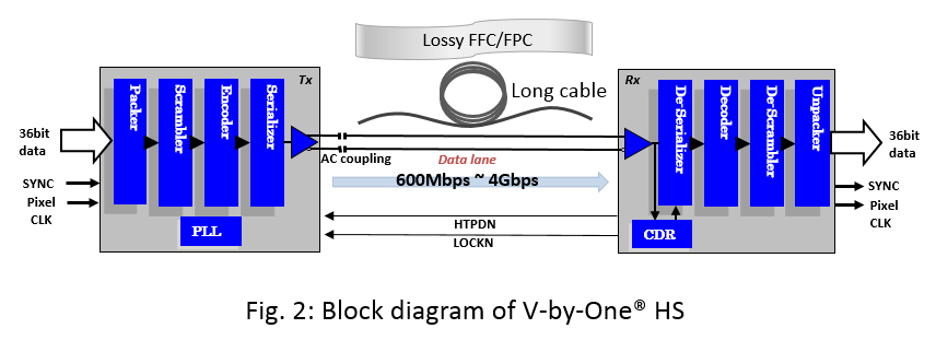
One of the main applications of V-by-One® HS is in automotive equipment (car cameras). Thanks to its very fast transmission data rate of 4 Gbps, V-by-One® HS can transmit high-resolution data as well as images taken by multiple cameras via one cable (Fig. 2). This reduces both cost and vehicle weight, while enhancing robustness.
Medical equipment, amusement equipment, and multifunctional printers also leverage V-by-One® HS as an interface for image/video signal transmission, especially transmission between two PCBs, an image sensor, and a controller or a PCB and LCD panel. V-by-One® HS provides positive effects in terms of higher resolution and faster frame rate, as well as a shorter cable length and smaller cable diameter.
Here is a specific example. Upon bridging an image sensor to a control board by V-by-One® HS, data can be transmitted even via copper cables 0.32 mm (AWG28) or 0.25 mm (AWG30) in diameter. Only V-by-One® HS enables the use of such thin cables several meters in length to transmit data. Thinner cables are flexible and easy for users to handle in a narrow space.
The data sheet of the SerDes chip supporting V-by-One® HS defines the names of such signals as DE (Data Enable), Hsync (Horizontal Synchronization), and Vsync (Vertical Synchronization), which control the transmission timing of image/video data. Therefore, some engineers may mistakenly think that V-by-One® HS is an interface dedicated to image/video data. Actually, V-by-One® HS is a common SerDes product with 8B/10B coding and widely suited for any type of data communication.
First, the Hsync and Vsync signals need not be used, as a device will only work with the DE signal used to insert K code (K28.5), which is one of the K codes and indicates the boundary of 10-bit signals. Again, just using DE as a control signal by inserting K28.5 is required for using V-by-One® HS as a general SerDes chip for data communication such as bus and data. V-by-One® HS is a “universal SerDes chip of up to 4-Gbps speed that adopts the 8B/10B coding method.”
V-by-One® HS PHY is similar to PCI Express Gen 2, which is also a clock-embedded technology using 8B/10B coding. The difference is that PCI Express Gen2 has a higher data transmission rate (5 Gbps) than that of V-by-One® HS (4Gbps) and must comply with the upper protocol layer.
Therefore, V-by-One® HS is more flexible than PCI Express when used as a high speed interface for general data communication. In addition, V-by-One® HS requires no handshaking processing and has no overhead. Furthermore, it can freely implement higher layer protocols as required.
Various types of V-by-One® HS
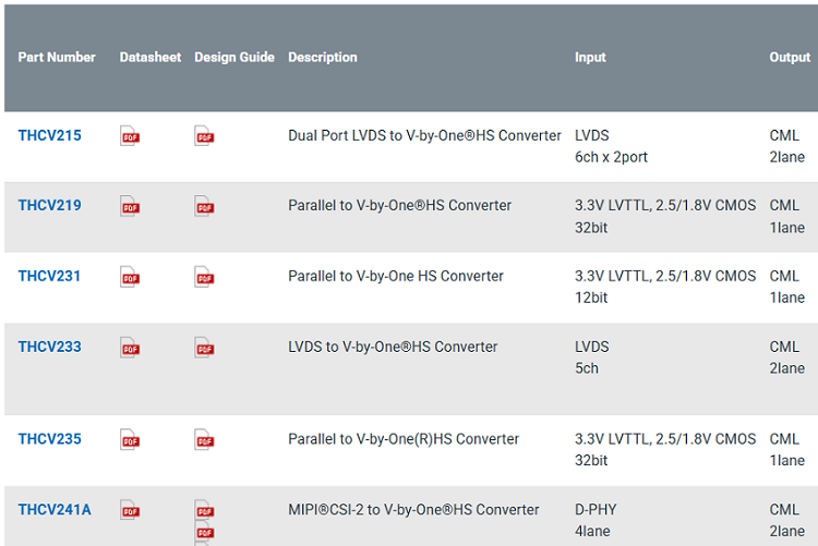
THine has already commercialized various types of V-by-One® HS transmitter/receiver ICs (Table 1).
Table1:List of V-by-One HS product lineup
THCV231 and THCV235 are transmitter ICs with the maximum data transmission rate per lane corresponding to the LVCMOS input signal of 4 Gbps (left side in Fig. 3). The clock frequency corresponds to a wide range from 24 M to 160 MHz. The interface of V-by-One® HS is basically one lane, though some products have multiple lanes, depending on the device. Users can select the interface according to the bandwidth required.

THCV231 and THCV235 differ in terms of their package. THCV231 is sealed in a 32-pin QFN, while THCV235 is placed in a 64-pin QFN. THCV231 was designed to be compatible with any electronic device requiring a small package. THCV236 is the receiver corresponding to these transmitters with the 64-pin QFN package (right side in Fig. 3), and outputs the LVCMOS signal.
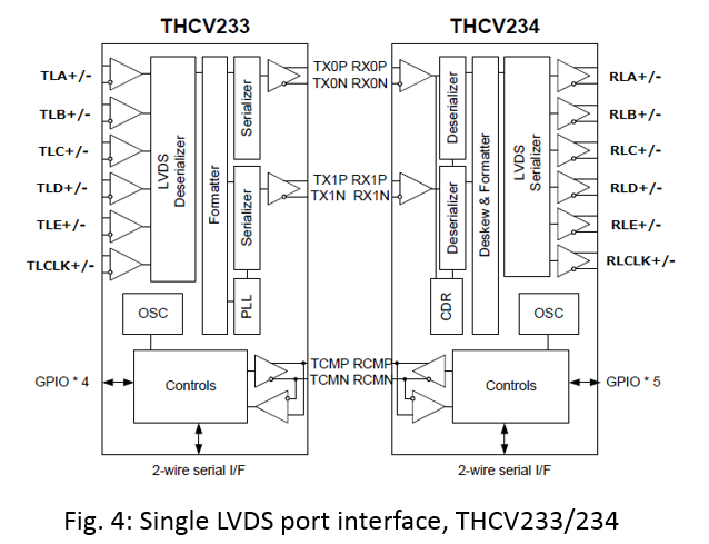
THine also provides transmitter/receiver ICs corresponding to the LVDS input and output signals of LVDS. THCV233 and THCV234 are a transmitter IC and a receiver IC corresponding to a single LVDS port and a single V-by-One® HS port, respectively (Fig. 4).
Their maximum data transmission rate is 3.4Gbps.
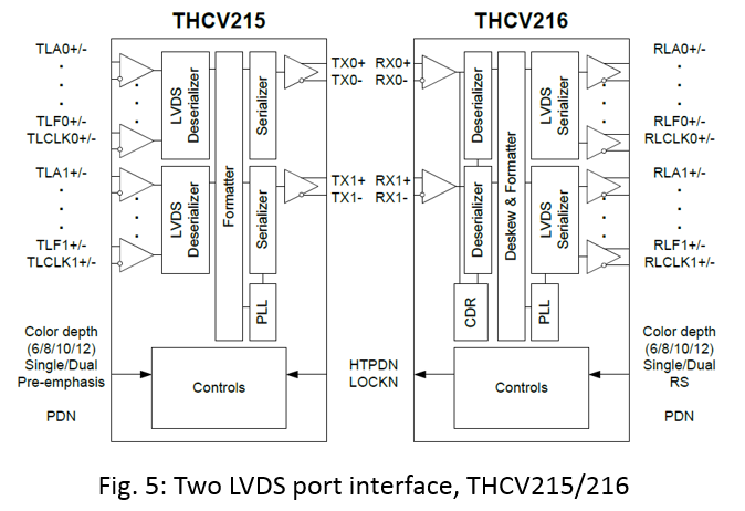
THCV215 and THCV216 are a transmitter IC and a receiver IC with two LVDS and two V-by-One® HS ports, respectively. The maximum data transmission rate is 3.75 Gbps per lane (Fig. 5).

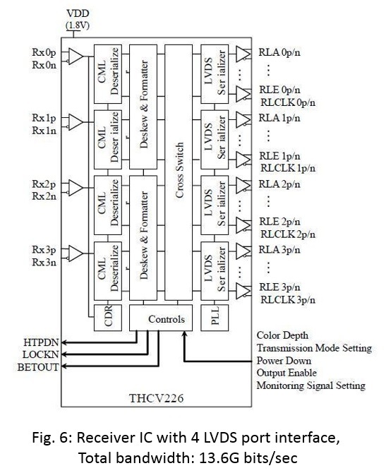
THCV226 is a receiver IC compatible with 4-port LVDS. Although THine does not offer a 4-port compatible transmitter IC with four output lanes, users can design transmission using four lanes by employing two serial output ICs, THCV215 or THCV217 (2-port output transmitter IC), or by integrating the transmitter circuits in ASIC. THCV226 covers a very wide bandwidth due to the four lanes and its maximum data transmission rate is 3.4 Gbps, in total, reaching 13.6 Gbps (active bandwidth at 10.88 Gbps).
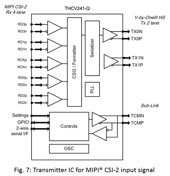
Recently THine released transmitter IC THCV241-Q compatible with MIPI® CSI-2 input signals. It has four input lanes of MIPI® CSI-2 and two output lanes for V-by-One® HS (Fig. 7). THCV241-Q was developed for environments where more automotive and surveillance cameras are gradually implementing MIPI® CSI-2 interfaces. THCV241-Q realizes longer cable length and fewer lanes.
The number of pixels actually becomes larger and the frame speed becomes much faster in many applications such as automotive cameras, surveillance cameras, and machine vision. Therefore, V-by-One® HS is not only for LCD-TVs, but will play a major role in a wide market.
THCV231 and THCV235 are transmitter ICs with the maximum data transmission rate per lane corresponding to the LVCMOS input signal of 4 Gbps (left side in Fig. 3). The clock frequency corresponds to a wide range from 24 M to 160 MHz. The interface of V-by-One® HS is basically one lane, though some products have multiple lanes, depending on the device. Users can select the interface according to the bandwidth required.
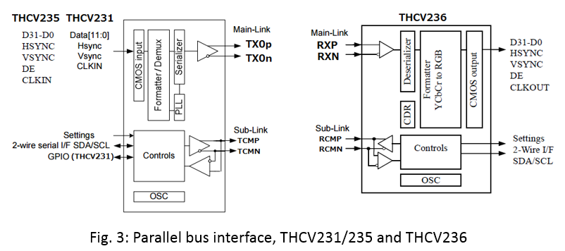
THCV231 and THCV235 differ in terms of their package. THCV231 is sealed in a 32-pin QFN, while THCV235 is placed in a 64-pin QFN. THCV231 was designed to be compatible with any electronic device requiring a small package. THCV236 is the receiver corresponding to these transmitters with the 64-pin QFN package (right side in Fig. 3), and outputs the LVCMOS signal.
THine also provides transmitter/receiver ICs corresponding to the LVDS input and output signals of LVDS. THCV233 and THCV234 are a transmitter IC and a receiver IC corresponding to a single LVDS port and a single V-by-One® HS port, respectively (Fig. 4).
Their maximum data transmission rate is 3.4Gbps.

THCV215 and THCV216 are a transmitter IC and a receiver IC with two LVDS and two V-by-One® HS ports, respectively. The maximum data transmission rate is 3.75 Gbps per lane (Fig. 5).
THCV226 is a receiver IC compatible with 4-port LVDS. Although THine does not offer a 4-port compatible transmitter IC with four output lanes, users can design transmission using four lanes by employing two serial output ICs, THCV215 or THCV217 (2-port output transmitter IC), or by integrating the transmitter circuits in ASIC. THCV226 covers a very wide bandwidth due to the four lanes and its maximum data transmission rate is 3.4 Gbps, in total, reaching 13.6 Gbps (active bandwidth at 10.88 Gbps).

Recently THine released transmitter IC THCV241-Q compatible with MIPI® CSI-2 input signals. It has four input lanes of MIPI® CSI-2 and two output lanes for V-by-One® HS (Fig. 7). THCV241-Q was developed for environments where more automotive and surveillance cameras are gradually implementing MIPI® CSI-2 interfaces. THCV241-Q realizes longer cable length and fewer lanes.

The number of pixels actually becomes larger and the frame speed becomes much faster in many applications such as automotive cameras, surveillance cameras, and machine vision. Therefore, V-by-One® HS is not only for LCD-TVs, but will play a major role in a wide market.
*“MIPI®” is a registered trademark of MIPI Alliance, Inc.
Related Contents
- The technology of V-by-One® SerDes apply not only to TV application but to high-speed interfaces for communication/computer/industrial equipment as well
- V-by-One® HS goes beyond LVDS -Long distance transmission at a high speed is achieved with high reliable 8B/10B coding and signal conditioning technology-
- Deep dive about the Basic Principle of LVDS SerDes, Taking advantage of its features – high speed, long distance, low noise
- History of THine products for signal transmission started from SerDes IC for laptop PC